SF32LB58x Hardware Design Guide
1. Introduction
This hardware design guide provides recommendations and reference material for products based on the SF32LB58x family of high-performance AIoT microcontrollers. It is intended for hardware engineers, PCB designers, and product developers building battery-powered products with rich user interfaces, large memory, dual-mode Bluetooth, audio, high GPIO count, and low-power standby requirements.
The guide covers the complete hardware development process, including PMIC and power distribution, BGA256 fanout, HDI stack-up planning, clock circuits, RF design, MIPI-DSI, USB2.0 High-Speed, SDIO/eMMC, audio circuits, PCB layout, validation, and manufacturing preparation. Following these guidelines helps reduce risk in dense BGA/HDI designs, protect signal integrity on high-speed interfaces, and keep the product aligned with the SF32LB58x power, package, and production requirements.
This document assumes a basic understanding of embedded hardware design, schematic capture, and high-density PCB layout. It complements the SF32LB58x datasheet, user manual, official hardware application note, reference design package, and SiFli Approved Vendor List, which remain the authority for electrical specifications, pin multiplexing, package dimensions, component qualification, and production limits.
2. Development Resources
3. Device Overview
3.1. Architecture
| Feature | Description |
|---|---|
| Core architecture | Heterogeneous triple-core architecture: 2x application Arm Cortex-M33 STAR-MC1 cores up to 240 MHz and 1x low-power Arm Cortex-M33 STAR-MC1 core up to 96 MHz |
| Bluetooth | Integrated low-power Bluetooth 6.3 transceiver |
| Graphics | ePicasso 2.0 2D/2.5D graphics acceleration and Vivante GCNanoUltraV vector graphics |
| Display interfaces | MIPI-DSI, SPI/QSPI, MCU8080, DPI, parallel/serial JDI |
| Storage | Model-dependent co-packaged NOR Flash/PSRAM, plus external MPI4, SD1, and SD2 interfaces |
| Audio | 3x I2S, 2x PDM, differential analog audio input/output, external analog audio PA and I2S audio PA support |
| Wake interrupts | 16 wake-capable interrupt sources in Standby/Hibernate mode: 6 on PA and 10 on PB |
| PBR interface | 6 general-purpose PBR pins for LSW control, 32 kHz clock output, or wake input |
3.2. Variants
Specific SF32LB58x ordering codes and co-packaged memory combinations should be confirmed from the latest datasheet and AVL before schematic freeze. From a board-design perspective, treat the whole SF32LB58x family as a BGA256, HDI-only platform with model-dependent SIP memory and external storage options through MPI4, SD1, and SD2.
3.3. Packages
| Package Name | Dimensions | Pin Pitch |
|---|---|---|
| BGA256 | 8.5 mm x 6.5 mm x 0.94 mm | 0.4 mm |
3.4. Major Hardware Features
- BGA256 package with 0.4 mm pitch and dense power/GPIO fanout.
- HDI PCB process required; the design is not PTH-compatible.
- Integrated PMU with 2 BUCK outputs and 3 internal LDO outputs.
- Optional system PMIC SF30147C for watch-class system power distribution.
- MIPI-DSI, USB2.0 HS, SDIO/eMMC, RF, audio, and dense BGA fanout require early stack-up and impedance confirmation.
3.5. Typical Applications
SF32LB58x is recommended for premium connected products that need advanced graphics, large memory, high GPIO count, multimedia, and edge AI capability, including:
- Premium smartwatches, sports watches, and outdoor wearables
- Advanced cycling computers and vehicle-mounted dashboards
- Smart displays and connected dashboards
- AI-enabled wearable devices
- Edge AI and sensor-fusion systems
- High-resolution LVGL-based HMI devices
- Portable medical and industrial terminals
- Bluetooth + Wi-Fi accessories that use an external SDIO Wi-Fi device
4. Design at a Glance
4.1. Hardware Architecture
| Design Item | Typical Implementation |
|---|---|
| Package | BGA256, 8.5 mm x 6.5 mm x 0.94 mm, 0.4 mm pitch |
| PCB | HDI board only — not PTH-compatible; 6HDI-2 stack-up recommended |
| Power Supply | Integrated PMU (2x BUCK + 3x LDO); optionally paired with SiFli's PMIC SF30147C for whole-system power |
| Buck Inductor | 4.7 uH, DCR ≤ 0.4 Ω, Isat ≥ 500 mA |
| Clock | 48 MHz main crystal + 32.768 kHz RTC crystal |
| RF | 50 Ω controlled-impedance trace, reserved π matching network |
| Display | MIPI-DSI (2-lane), 3/4-wire SPI, Quad-SPI, MCU8080, DPI, parallel/serial JDI; dual LCDC1 (PA) / LCDC2 (PB) pin mapping |
| Storage | MPI4 for external SPI NAND Flash; dual SD1/SD2 SDIO interfaces for eMMC, SD NAND, or SD card |
| Audio | 3x I2S (master-only), 2x PDM, differential analog audio input/output |
| Debug | 1x SWD + 6x selectable UART debug outputs |
| USB | USB2.0 HS, Host/Device modes |
4.2. Hardware Design Flow
| Step | Design Decision | Primary Sections |
|---|---|---|
| 1 | Confirm ordering code, SIP memory configuration, and BGA256 package assumptions | Device Overview, Packages |
| 2 | Freeze HDI stack-up, via structure, impedance rules, and assembly capability before layout starts | PCB Layout Guidelines |
| 3 | Define the SF30147C/system PMIC strategy, chip PMU rails, BUCK inductors, LDO capacitors, reset, and power sequencing | Power System |
| 4 | Select boot storage, display interface, USB role, SDIO/eMMC usage, audio topology, and debug access | Storage and Connectivity, User Interfaces, Manufacturing |
| 5 | Review clock, RF, DSI, USB2.0 HS, SDIO/eMMC, audio, DC/DC, BGA fanout, and ESD routing screenshots | Clock Generation, RF, PCB Layout Guidelines |
| 6 | Archive schematic, stack-up, DRC, impedance, AVL, manufacturing, and focused layout evidence before prototype release | Design Review Checklist |
4.3. How to Use This Guide
Use this guide in board-review order: confirm the package and SIP-memory configuration, lock the HDI stack-up and PMIC strategy, review boot storage and display routing, then verify clocks, RF, USB, audio, debug, and production test access. Section 5 is the schematic baseline, Section 6 is the PCB implementation baseline, and Section 7 is the release checklist.
4.4. Review Evidence Pack
Before prototype release, archive the schematic PDF, PCB stack-up, via/process capability statement, impedance report, DRC report, AVL cross-check, and focused layout screenshots for the PMIC, BUCK inductors, DSI, USB, SDIO/eMMC, RF, crystals, audio, BGA fanout, ground return, and ESD entry points.
5. Schematic Design Guidelines
This chapter groups the SF32LB58x schematic topics by engineering function: power, clock generation, RF, user interfaces, storage and connectivity, and manufacturing support. Each subsection starts from the design intent, then captures the circuit requirements, common risks, and release checks for the SF32LB58x platform.
| Group | Main Decisions | Release Evidence |
|---|---|---|
| Power System | System PMIC, chip PMU rails, BUCK inductors, LDO capacitors, reset, low-power wake sources | Power tree, PMIC settings, rail measurements, POR/BOR/reset review |
| Clock Generation | 48 MHz and 32.768 kHz crystals | Crystal specification check, matching-capacitor plan, crystal layout screenshots |
| RF | RF matching and antenna path | Impedance plan, RF matching network, antenna keep-out, layout screenshots |
| User Interfaces | Display, touch/backlight, audio, buttons, motor, PBR control | Interface schematics, pin assignments, power sequencing, analog/audio review |
| Storage and Connectivity | Boot mode, MPI4, SD1/SD2, eMMC/SD NAND/SD card, USB2.0 HS | Boot configuration, storage power plan, differential/high-speed routing evidence |
| Manufacturing | SWD, UART debug outputs, production test access, schematic/PCB checklist | Test-point drawing, recovery path, production flashing/calibration plan |
5.1. Power System
5.1.1. Power Supply
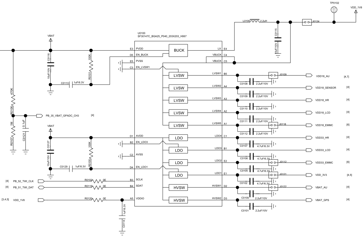
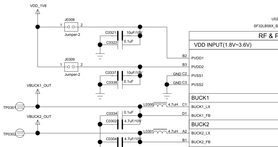
The SF32LB58x series has a built-in PMU power unit supporting 2 BUCK outputs, which require an external inductor and capacitor returning to the internal power input, plus 3 internal LDO outputs that require external capacitors. For watch-class designs, the SF32LB58x can be paired with SiFli's PMIC chip SF30147C, which supplies power to both the SF32LB58x and its associated peripherals.
5.1.1.1. SiFli PMIC Power Distribution
The SF30147C is a highly integrated, high-efficiency power management chip for ultra-low-power wearable products. It integrates 4 LDOs, each with a wide input/output voltage range and up to 100 mA load current. For different peripherals, the SF30147C integrates 7 low-leakage, low-Ron load switches: 2 high-voltage switches for peripherals driven directly from battery voltage (such as an audio PA), and 5 low-voltage switches for 1.8 V-powered peripherals. The SF32LB58x uses two GPIOs to emulate a TWI signal to control the SF30147C.
| SF30147C Power Pin | Min Voltage (V) | Max Voltage (V) | Max Current (mA) | Description |
|---|---|---|---|---|
| VBUCK | 1.8 | 1.8 | 500 | Powers the SF32LB58x's PVDD1, PVDD2, VDDIOA, VDDIOA2, VDDIOB, AVDD_BRF, AVDD18_DSI, and other 1.8 V rails |
| LVSW1 | 1.8 | 1.8 | 100 | I2S Class-K PA logic supply |
| LVSW2 | 1.8 | 1.8 | 100 | G-sensor 1.8 V supply |
| LVSW3 | 1.8 | 1.8 | 150 | Heart-rate sensor 1.8 V supply |
| LVSW4 | 1.8 | 1.8 | 150 | LCD 1.8 V supply |
| LVSW5 | 1.8 | 1.8 | 150 | eMMC core supply |
| LDO1 | 2.8 | 3.3 | 100 | Powers the SF32LB58x's AVDD33_USB, AVDD33_ANA, AVDD33_AUD, AVDDIOA2, and other 3.3 V rails |
| LDO2 | 2.8 | 3.3 | 100 | eMMC or SD NAND supply |
| LDO3 | 2.8 | 3.3 | 100 | LCD 3.3 V supply |
| LDO4 | 2.8 | 3.3 | 100 | Heart-rate sensor 3.3 V supply |
| HVSW1 | 2.8 | 5 | 150 | Analog Class-K PA supply |
| HVSW2 | 2.8 | 5 | 150 | GPS supply |
Refer to the SF30147C chip datasheet for full details.
5.1.1.2. SF32LB58x Power Requirements
The SF32LB58x series integrates the following PMU power specifications.
| PMU Power Pin | Min Voltage (V) | Typ Voltage (V) | Max Voltage (V) | Max Current (mA) | Description |
|---|---|---|---|---|---|
| PVDD1 | 1.71 | 1.8 | 3.6 | 100 | PVDD1 power input |
| PVDD2 | 1.71 | 1.8 | 3.6 | 50 | PVDD2 power input |
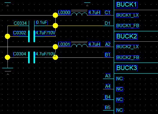
| BUCK1_LX / BUCK1_FB | - | 1.25 | - | 100 | BUCK1_LX output connects to the inductor and internal power input 1; the other end of the inductor connects to an external capacitor |
| BUCK2_LX / BUCK2_FB | - | 0.9 | - | 50 | BUCK2_LX output connects to the inductor and internal power input 2; the other end of the inductor connects to an external capacitor |
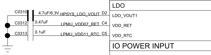
| LDO_VOUT1 | - | 1.1 | - | 100 | LDO output, external capacitor required |
| VDD_RET | - | 0.9 | - | 1 | RET LDO output, external capacitor required |
| VDD_RTC | - | 1.1 | - | 1 | RTC LDO output, external capacitor required |
| MIC_BIAS | 1.4 | - | 2.8 | - | Microphone power output |
Other power pins requiring external supply are specified below.
| Other Power Pin | Min Voltage (V) | Typ Voltage (V) | Max Voltage (V) | Max Current (mA) | Description |
|---|---|---|---|---|---|
| AVDD_BRF | 1.71 | 1.8 | 3.3 | 1 | RF power input |
| AVDD18_DSI | 1.71 | 1.8 | 2.5 | 20 | MIPI DSI power input; leave floating if unused |
| AVDD33_ANA | 3.15 | 3.3 | 3.45 | 50 | Analog power + RF PA power input |
| AVDD33_AUD | 3.15 | 3.3 | 3.45 | 50 | Analog audio power input |
| AVDD33_USB | 3.15 | 3.3 | 3.45 | 50 | USB power input |
| VDDIOA | 1.71 | 1.8 | 3.45 | - | PA12-PA93 I/O power input |
| VDDIOA2 | 1.71 | 1.8 | 3.45 | - | PA0-PA11 I/O power input |
| VDDIOB | 1.71 | 1.8 | 3.45 | - | PB I/O power input |
| VDDIOSA | 1.71 | 1.8 | 1.98 | - | SIPA power input |
| VDDIOSB | 1.71 | 1.8 | 1.98 | - | SIPB power input |
| VDDIOSC | 1.71 | 1.8 | 1.98 | - | SIPC power input |
| GPADC_VREFP | - | - | - | - | GPADC reference voltage input; capacitor only, no external supply |
| AUD_VREF | - | - | - | - | Audio reference voltage input; capacitor only, no external supply |
5.1.1.3. Recommended Capacitor Values
| Power Pin | Capacitor | Description |
|---|---|---|
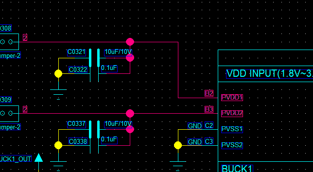
| PVDD1 | 0.1 uF + 10 uF | Place at least 10 uF and 0.1 uF (2 capacitors total) close to the pin |
| PVDD2 | 0.1 uF + 10 uF | Place at least 10 uF and 0.1 uF (2 capacitors total) close to the pin |
| BUCK1_LX / BUCK1_FB | 0.1 uF + 4.7 uF | Place at least 4.7 uF and 0.1 uF (2 capacitors total) close to the pin |
| BUCK2_LX / BUCK2_FB | 0.1 uF + 4.7 uF | Place at least 4.7 uF and 0.1 uF (2 capacitors total) close to the pin |
| LDO_VOUT1 | 4.7 uF | Place at least one 4.7 uF capacitor close to the pin |
| VDD_RET | 0.47 uF | Place at least one 0.47 uF capacitor close to the pin |
| VDD_RTC | 0.1 uF | Place at least one 0.1 uF capacitor close to the pin |
| AVDD_BRF | 1 uF | Place at least one 1 uF capacitor close to the pin |
| AVDD18_DSI | 4.7 uF | Place at least one 4.7 uF capacitor close to the pin |
| AVDD33_ANA | 1 uF | Place at least one 1 uF capacitor close to the pin |
| AVDD33_AUD | 4.7 uF | Place at least one 4.7 uF capacitor close to the pin |
| AVDD33_USB | 1 uF | Place at least one 1 uF capacitor close to the pin |
| MIC_BIAS | 1 uF | Place at least one 1 uF capacitor close to the pin |
| VDDIOA / VDDIOA2 / VDDIOB | 1 uF | Place at least one 1 uF capacitor close to the pin |
| VDDIOSA / VDDIOSB / VDDIOSC | 1 uF | Place at least one 1 uF capacitor close to the pin |
5.1.1.4. BUCK Inductor Selection
Key power inductor parameters
L (inductance) = 4.7 uH, DCR (DC resistance) ≤ 0.4 Ω, Isat (saturation current) ≥ 500 mA
5.1.1.5. Power-Up Sequencing and Reset
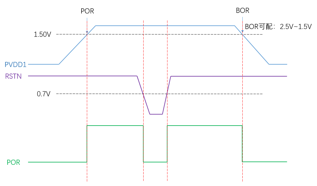
The SF32LB58x series has built-in POR (Power-On Reset) and BOR (Brownout Reset), and also supports an external hardware reset signal, RSTN.
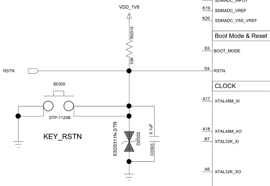
The RSTN reset signal should be pulled up to the PVDD1 input voltage domain, with a 0.1 uF capacitor to ground forming an RC delayed reset.
5.1.1.6. Typical Power Circuit
The SF32LB58x series can use SiFli's PMIC SF30147C to supply its power rails; see Table 5-1 for the assignment. The chip package also has 2 built-in BUCK outputs and 3 built-in LDO outputs.
5.1.1.7. Power Design Checklist
- Confirm the selected model's PVDD1/PVDD2 supply range (1.71 V–3.6 V) matches the actual power scheme
- BUCK inductor meets 4.7 uH, DCR ≤ 0.4 Ω, Isat ≥ 500 mA
- PVDD1/PVDD2, BUCK1/2_LX/FB, LDO_VOUT1, VDD_RET, and VDD_RTC decoupling capacitors use the recommended values listed in this section
- If using SF30147C, the voltage/current allocation of the 7 load switches matches peripheral requirements
- The RSTN reset circuit's RC delay meets the device's reset timing requirements
5.1.2. Operating Modes and Wake Sources
The low-power strategy should be reviewed together with PBR functions, wake-capable interrupts, storage power switches, sensor supplies, and external PMIC load switches.
The SF32LB58x series provides 6 PBR interfaces, with these key characteristics:
- PBR0 transitions from 0 to 1 during power-up, useful for driving certain external LSWs; PBR1-PBR5 default to output 0;
- PBR0-PBR5 can all act as outputs in both Standby and Hibernate modes;
- PBR0-PBR5 can output the LPTIM signal;
- PBR0-PBR5 can output a 32 kHz clock signal;
- PBR0-PBR3 can be configured as inputs for wake-up signal input — the MCU does not receive an interrupt while it is awake.
All GPIOs on the SF32LB58x series support wake-up in light/deep sleep mode. In Standby and Hibernate modes, 16 wake-capable interrupt sources are supported — 6 on PA and 10 on PB.
| Interrupt Source | I/O | Description |
|---|---|---|
| WKUP_PIN0 | PB54 | Interrupt signal 0 |
| WKUP_PIN1 | PB55 | Interrupt signal 1 |
| WKUP_PIN2 | PB56 | Interrupt signal 2 |
| WKUP_PIN3 | PB57 | Interrupt signal 3 |
| WKUP_PIN4 | PB58 | Interrupt signal 4 |
| WKUP_PIN5 | PB59 | Interrupt signal 5 |
| WKUP_PIN6 | PA64 | Interrupt signal 6 |
| WKUP_PIN7 | PA65 | Interrupt signal 7 |
| WKUP_PIN8 | PA66 | Interrupt signal 8 |
| WKUP_PIN9 | PA67 | Interrupt signal 9 |
| WKUP_PIN10 | PA68 | Interrupt signal 10 |
| WKUP_PIN11 | PA69 | Interrupt signal 11 |
| WKUP_PIN12 | PBR0 | Interrupt signal 12 |
| WKUP_PIN13 | PBR1 | Interrupt signal 13 |
| WKUP_PIN14 | PBR2 | Interrupt signal 14 |
| WKUP_PIN15 | PBR3 | Interrupt signal 15 |
5.2. Clock Generation
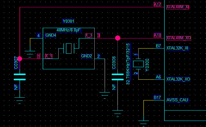
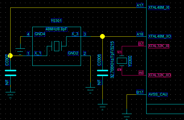
The SF32LB58x series requires 2 external clock sources: a 48 MHz main crystal and a 32.768 kHz RTC crystal.
| Crystal | Specification | Description |
|---|---|---|
| 48 MHz | 7 pF ≤ CL ≤ 12 pF (recommended 8.8 pF), ΔF/F0 ≤ ±10 ppm, ESR ≤ 30 Ω (recommended 22 Ω) | Crystal power consumption correlates with CL and ESR — smaller values give lower power. Reserve parallel matching capacitors next to the crystal; not required when CL < 12 pF |
| 32.768 kHz | CL ≤ 12.5 pF (recommended 7 pF), ΔF/F0 ≤ ±20 ppm, ESR ≤ 80 kΩ (recommended 38 kΩ) | Crystal power consumption correlates with CL and ESR — smaller values give lower power. Reserve parallel matching capacitors next to the crystal; not required when CL < 12.5 pF |
| Model | Vendor | Parameters |
|---|---|---|
| E1SB48E001G00E | Hosonic | F0 = 48.000000 MHz, ΔF/F0 = -6 ~ 8 ppm, CL = 8.8 pF, ESR ≤ 22 Ω Max, TOPR = -30 ~ 85°C, Package 2016 (metric) |
| ETST00327000LE | Hosonic | F0 = 32.768 kHz, ΔF/F0 = -20 ~ 20 ppm, CL = 7 pF, ESR ≤ 70 kΩ Max, TOPR = -40 ~ 85°C, Package 3215 (metric) |
| SX20Y048000B31T-8.8 | TKD | F0 = 48.000000 MHz, ΔF/F0 = -10 ~ 10 ppm, CL = 8.8 pF, ESR ≤ 40 Ω Max, TOPR = -20 ~ 75°C, Package 2016 (metric) |
| SF32K32768D71T01 | TKD | F0 = 32.768 kHz, ΔF/F0 = -20 ~ 20 ppm, CL = 7 pF, ESR ≤ 70 kΩ Max, TOPR = -40 ~ 85°C, Package 3215 (metric) |
Note
SX20Y048000B31T-8.8 has a slightly larger ESR, which also slightly increases static power consumption. When routing the PCB, remove the layer-2 GND copper directly beneath the crystal to reduce parasitic load capacitance on the clock signal.
See the SiFli Approved Vendor List for detailed qualified-material information.
5.3. RF
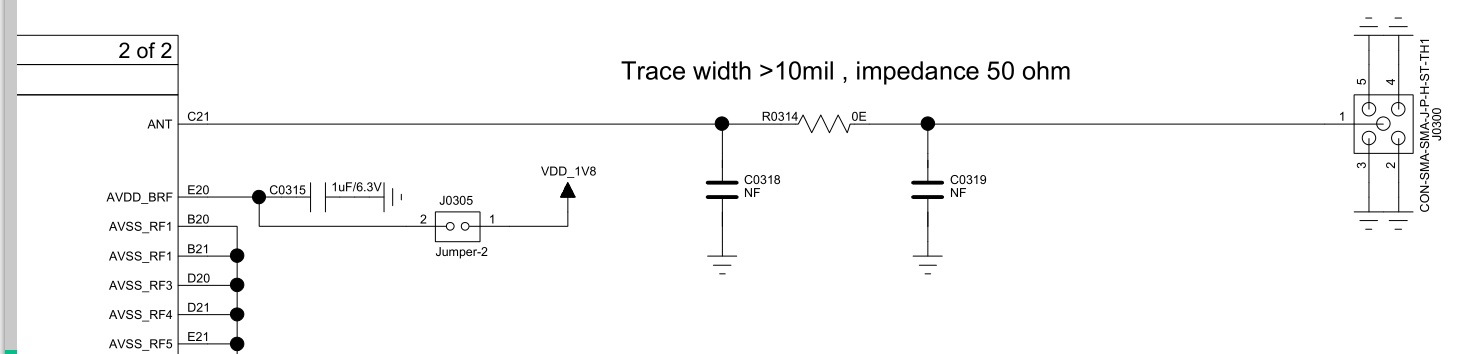
The SF32LB58x's RF front end uses on-chip integrated wideband matching-filter technology, so only a 50 Ω controlled-impedance RF PCB trace is required. A π-matching network for spurious filtering and antenna matching should be reserved in the design.
Note
The component values in the matching network must be determined by testing against the actual antenna and PCB layout.
5.4. User Interfaces
5.4.1. Display
5.4.1.1. MIPI DSI Display Interface
The SF32LB58x series supports a 2-lane MIPI DSI display interface.
| MIPI DSI Signal | I/O | Description |
|---|---|---|
| CLKP | DSI_CLKP | MIPI clock signal + |
| CLKN | DSI_CLKN | MIPI clock signal - |
| D0P | DSI_D0P | MIPI data lane 0 + |
| D0N | DSI_D0N | MIPI data lane 0 - |
| D1P | DSI_D1P | MIPI data lane 1 + |
| D1N | DSI_D1N | MIPI data lane 1 - |
| - | AVDD18_DSI | MIPI power input |
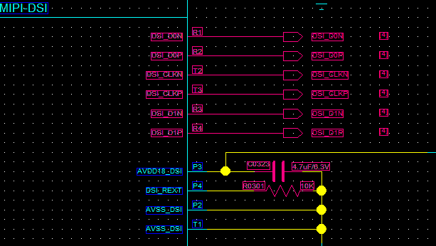
| - | DSI_REXT | External 10 kΩ resistor to ground |
| - | AVSS_DSI | Ground |
| TE | PB2 | Tearing effect to MCU frame signal |
| RESET | PB5 | Display reset signal |
5.4.1.2. SPI/QSPI Display Interface
The SF32LB58x series supports 3/4-wire SPI and Quad-SPI interfaces for connecting an LCD panel — the big core uses LCDC1 on PA, the little core uses LCDC2 on PB.
| SPI Signal | I/O (LCDC1) | I/O (LCDC2) | Description |
|---|---|---|---|
| CSX | PA44 | PB08 | Chip enable |
| WRX_SCL | PA46 | PB10 | Clock signal |
| DCX | PA48 | PB03 | Data/command signal in 4-wire SPI mode; data 1 in Quad-SPI mode |
| SDI_RDX | PA50 | PB09 | Data input in 3/4-wire SPI mode; data 0 in Quad-SPI mode |
| SDO | PA50 | PB09 | Data output in 3/4-wire SPI mode; tie together with SDI_RDX |
| D[0] | PA47 | PB04 | Data 2 in Quad-SPI mode |
| D[1] | PA45 | PB06 | Data 3 in Quad-SPI mode |
| REST | PA74 | PB05 | Display reset signal |
| TE | PA43 | PB02 | Tearing effect to MCU frame signal |
5.4.1.3. MCU8080 Display Interface
The SF32LB58x series supports an MCU8080 interface for connecting an LCD panel.
| MCU8080 Signal | I/O | Description |
|---|---|---|
| CSX | PA44 | Chip select |
| WRX | PA46 | Write strobe signal for write data |
| DCX | PA48 | Display data / command selection |
| RDX | PA50 | Read strobe signal for write data |
| D[0] | PA47 | Data 0 |
| D[1] | PA45 | Data 1 |
| D[2] | PA26 | Data 2 |
| D[3] | PA27 | Data 3 |
| D[4] | PA42 | Data 4 |
| D[5] | PA51 | Data 5 |
| D[6] | PA52 | Data 6 |
| D[7] | PA58 | Data 7 |
| REST | PA24 | Reset |
| TE | PA43 | Tearing effect to MCU frame signal |
5.4.1.4. DPI Display Interface
The SF32LB58x series supports a DPI interface for connecting an LCD panel.
| DPI Signal | I/O | Description |
|---|---|---|
| CLK | PA12 | Clock signal |
| DE | PA13 | Data-enable signal |
| HSYNC | PA14 | Horizontal sync signal |
| VSYNC | PA15 | Vertical sync signal |
| SD | PA18 | Display shutdown control |
| CM | PA19 | Switches between Normal Color and Reduced Color mode |
| R0-R7 | PA22/PA23/PA24/PA25/PA26/PA27/PA43/PA44 | Pixel data (red R0-R7) |
| G0-G7 | PA45/PA46/PA47/PA48/PA50/PA53/PA54/PA55 | Pixel data (green G0-G7) |
| B0-B7 | PA56/PA57/PA58/PA61/PA62/PA63/PA65/PA67 | Pixel data (blue B0-B7) |
5.4.1.5. JDI Display Interface
The SF32LB58x series supports both parallel and serial JDI interfaces for connecting an LCD panel, multiplexed onto either LCDC1 (PA) or LCDC2 (PB) signals — LCDC2 (PB) is recommended.
| JDI Signal | I/O (LCDC1) | I/O (LCDC2) | Description |
|---|---|---|---|
| JDI_VCK | PA19 | PB15 | Shift clock for the vertical driver |
| JDI_VST | PA22 | PB19 | Start signal for the vertical driver |
| JDI_XRST | PA25 | PB16 | Reset signal for the horizontal and vertical driver |
| JDI_HCK | PA43 | PB05 | Shift clock for the horizontal driver |
| JDI_HST | PA44 | PB10 | Start signal for the horizontal driver |
| JDI_ENB | PA45 | PB12 | Write enable signal for the pixel memory |
| JDI_R1 | PA46 | PB09 | Red image data (odd pixels) |
| JDI_R2 | PA47 | PB06 | Red image data (even pixels) |
| JDI_G1 | PA48 | PB08 | Green image data (odd pixels) |
| JDI_G2 | PA50 | PB04 | Green image data (even pixels) |
| JDI_B1 | PA65 | PB02 | Blue image data (odd pixels) |
| JDI_B2 | PA67 | PB03 | Blue image data (even pixels) |
| JDI_XFRP | PBR1 | PBR1 | Liquid crystal driving signal ("on" pixel) |
| JDI_VCOM/FRP | PBR2 | PBR2 | Common electrode driving signal / liquid crystal driving signal ("off" pixel) |
| JDI Signal | I/O (LCDC1) | I/O (LCDC2) | Description |
|---|---|---|---|
| JDI_SCS | PA82 | PB03 | Chip select signal |
| JDI_SCLK | PA84 | PB02 | Serial clock signal |
| JDI_SO | PA86 | PB06 | Serial data output signal |
| JDI_DISP | PA90 | PB04 | Display ON/OFF switching signal |
| JDI_EXTCOMIN | PA91 | PB05 | COM inversion polarity input |
5.4.2. Touch and Backlight
The SF32LB58x series supports an I2C-format touch controller interface with a touch-status interrupt input, plus 1 PWM signal to control backlight-driver enable and brightness.
| Touch/Backlight Signal | I/O | Description |
|---|---|---|
| Interrupt | PA69 | Touch status interrupt (wake-capable) |
| I2C1_SCL | PA17 | Touch panel I2C clock |
| I2C1_SDA | PA16 | Touch panel I2C data |
| BL_PWM | PB44 | Backlight PWM control signal |
| Reset | PA15 | Touch reset signal |
| Power Enable | PA12 | Touch panel power enable signal |
5.4.3. Audio
The SF32LB58x series provides a variety of audio-related interfaces, with the following characteristics:
- Supports 3 groups of I2S; I2S1 is input-only, while I2S2 and I2S3 support both input and output. All 3 I2S groups only support Master mode, not Slave mode;
- I2S1 is recommended for an I2S MIC input;
- I2S2 is recommended for an audio DAC;
- I2S3 is recommended for an audio codec;
- Supports 2 PDM MIC inputs;
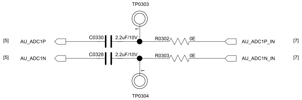
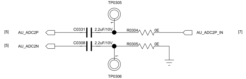
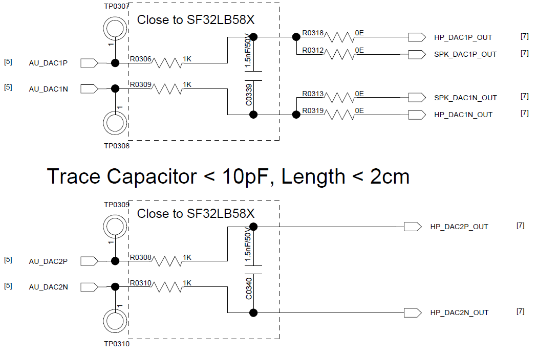
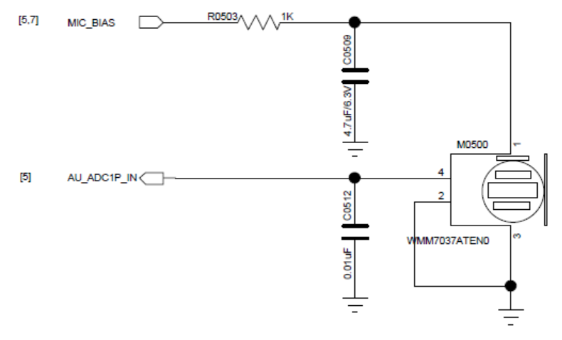
- Supports 2 analog MIC inputs, each requiring a DC-blocking capacitor of at least 2.2 uF; analog MIC power is supplied from the SF32LB58x's MIC_BIAS;
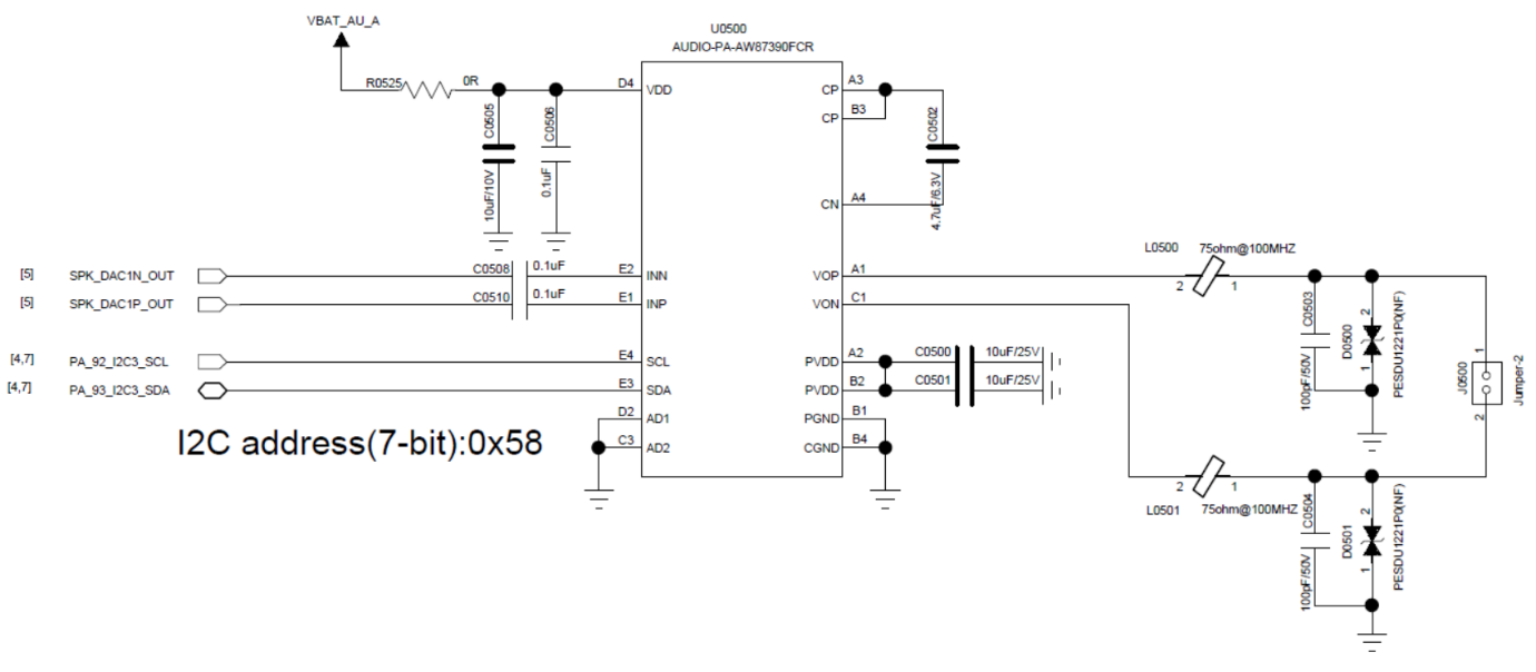
- Supports an external analog audio PA — both DAC output traces should be routed as differential pairs with 3D shielding, and additionally satisfy: trace parasitic capacitance < 10 pF, trace length < 2 cm;
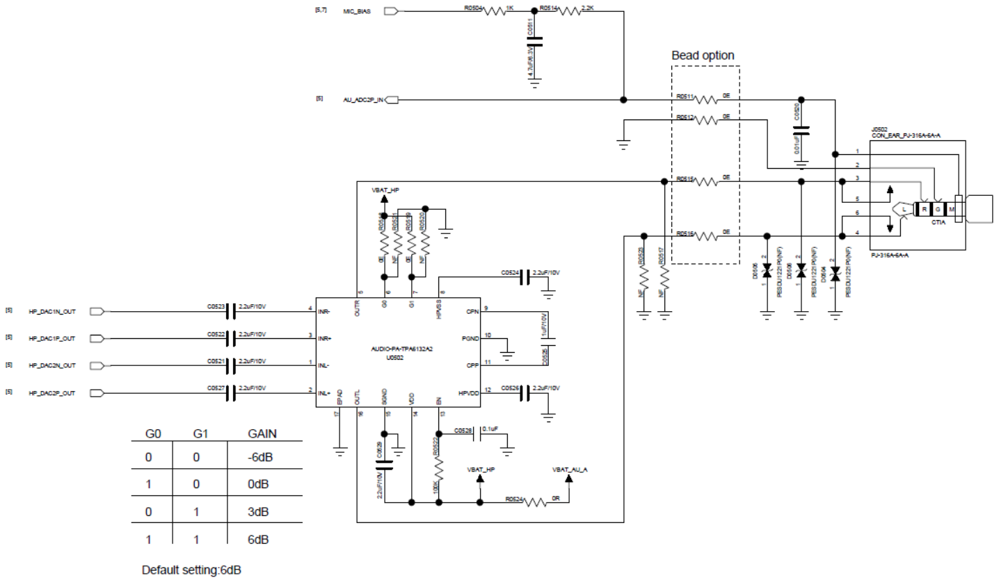
- Supports stereo analog headphone connection.
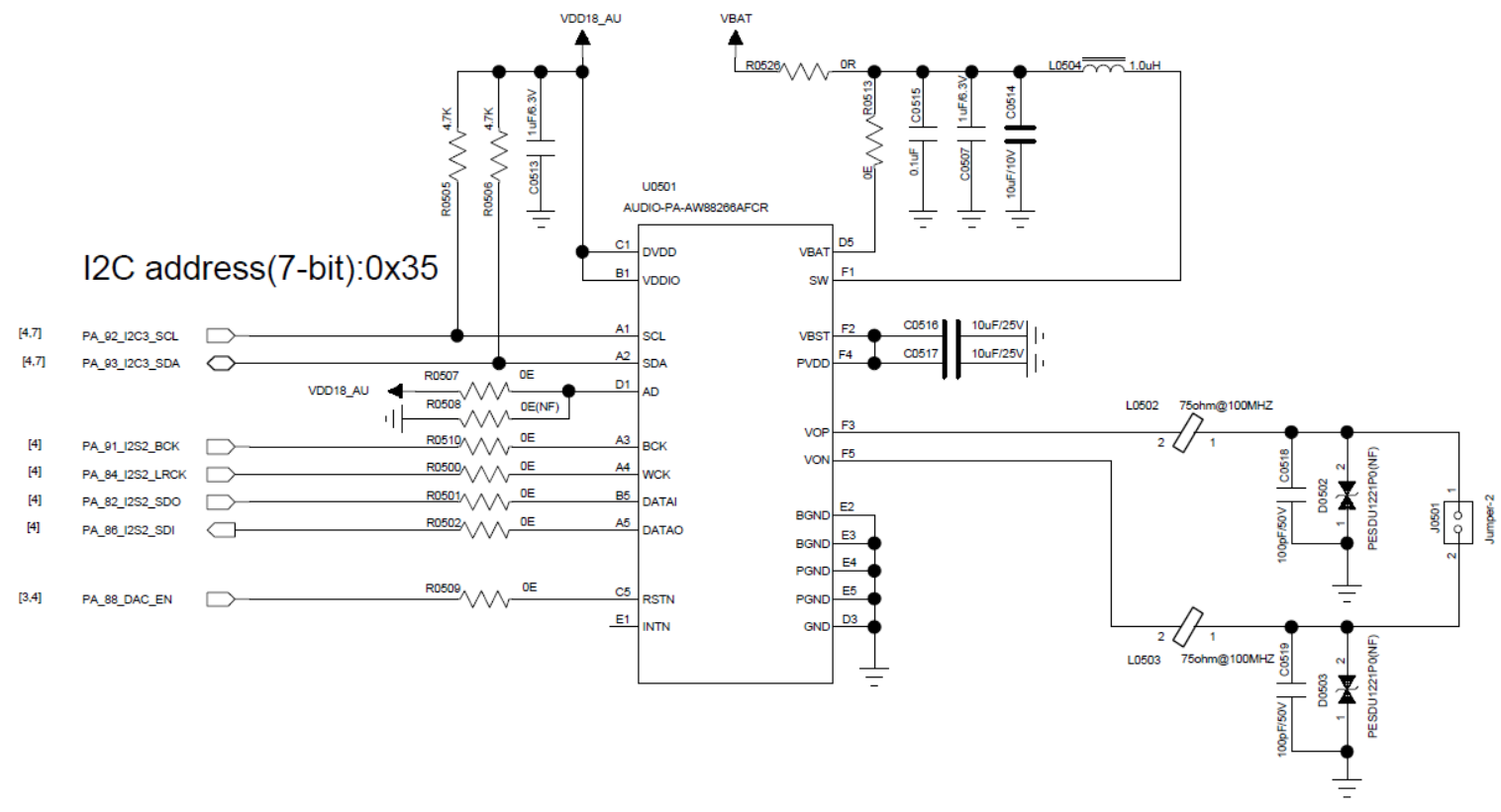
| Audio Signal | I/O | Description |
|---|---|---|
| I2S1_LRCK | PA14 | I2S1 frame clock |
| I2S1_SDI | PA18 | I2S1 data input |
| I2S1_BCK | PA23 | I2S1 bit clock |
| I2S2_LRCK | PA84 | I2S2 frame clock |
| I2S2_SDI | PA86 | I2S2 data input |
| I2S2_SDO | PA82 | I2S2 data output |
| I2S2_BCK | PA91 | I2S2 bit clock |
| I2S3_LRCK | PB31 | I2S3 frame clock |
| I2S3_SDI | PB27 | I2S3 data input |
| I2S3_SDO | PB24 | I2S3 data output |
| I2S3_BCK | PB30 | I2S3 bit clock |
| I2S3_MCLK | PB34 | I2S3 master clock |
| PDM1_CLK | PA23 | PDM1 clock |
| PDM1_DATA | PA18 | PDM1 data |
| PDM2_CLK | PA25 | PDM2 clock |
| PDM2_DATA | PA22 | PDM2 data |
| AU_ADC1P/AU_ADC1N | ADC1P/ADC1N | Analog input 1P/1N |
| AU_ADC2P/AU_ADC2N | ADC2P/ADC2N | Analog input 2P/2N |
| AU_DAC1P/AU_DAC1N | DAC1P/DAC1N | Analog output 1P/1N |
| AU_DAC2P/AU_DAC2N | DAC2P/DAC2N | Analog output 2P/2N |
Pin-multiplexing note
I2S1_SDI shares PA18 with PDM1_DATA, and I2S1_BCK shares PA23 with PDM1_CLK. I2S1_LRCK uses PA14, while PDM2_DATA uses PA22. Confirm the active audio function in the software interface configuration before finalizing the schematic.
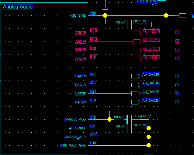
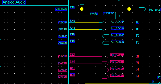
The SF32LB58x's analog MIC input supports both single-ended and differential modes, with a series 2.2 uF capacitor in either case; AU_ADC1P/AU_ADC1N/AU_ADC2P/AU_ADC2N connect to the SF32LB58x side. On the analog output side, AU_DAC1P/AU_DAC1N/AU_DAC2P/AU_DAC2N are SF32LB58x outputs that can drive either a stereo headphone PA input or an external analog audio PA input. Both the analog audio PA and the I2S audio PA are configured over I2C3.
5.4.4. Buttons
5.4.4.1. Power and Long-Press-Reset Button
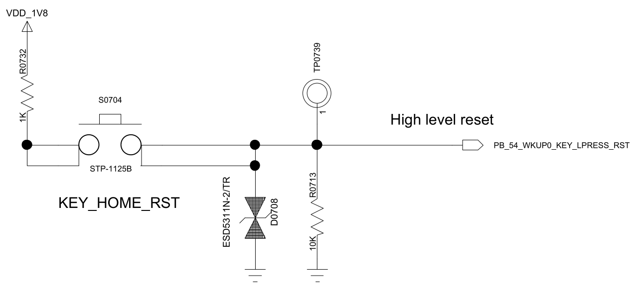
PB54 is the recommended power-key signal for the SF32LB58x series, combining a short-press power on/off function and a long-press reset function on a single button. The design is active-high; holding the button for more than 10 seconds triggers an automatic chip reset.
5.4.4.2. Function Button or Rotary Encoder
The SF32LB58x series supports function-button input and rotary-encoder signal input, both of which need to be pulled up. It also supports a light-tracking sensor, recommended over the I2C4 interface.
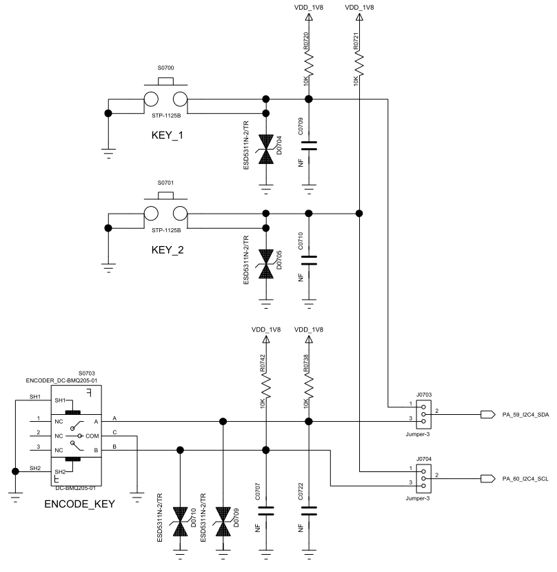
| I2C Signal | I/O | Description |
|---|---|---|
| INT | PA58 | Light-tracking sensor interrupt input |
| SDA | PA59 | Light-tracking sensor I2C data |
| SCL | PA60 | Light-tracking sensor I2C clock |
5.4.5. Vibration Motor
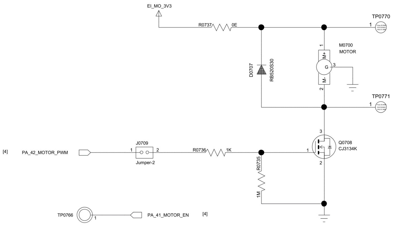
The SF32LB58x series supports multiple PWM outputs, which can drive a vibration motor.
Important
If the software enables the HCPU frequency-scaling macro #define BSP_PM_FREQ_SCALING 1, the HCPU clock drops when it enters the idle thread, and the PWM frequency on the corresponding PA pins changes accordingly. It is therefore recommended to output the PWM signal on a PB pin instead.
5.5. Storage and Connectivity
5.5.1. Boot Configuration
The SF32LB58x series provides a Mode pin to configure the boot mode.
| Mode Setting | Description |
|---|---|
| High | Enters download mode after power-up |
| Low | Jumps to the user application area after power-up |
Notes
- The Mode pin's voltage domain is the same as VDDIOA;
- Pull Mode to supply or GND through a 10 kΩ resistor to keep the level stable — it must not float or toggle;
- A test point for the Mode pin must be reserved on production boards for firmware download and crystal calibration; a jumper is not required;
- On test boards, it is recommended to reserve a jumper for the Mode pin so the board can be started in download mode after a firmware crash.
5.5.2. Storage
The SF32LB58x series supports MPI3 or MPI4 interfaces for external NOR Flash and SPI NAND Flash, and an SD1 interface for external SD NAND and eMMC.
5.5.2.1. QSPI NAND Flash Interface
The SF32LB58x EVB reference board uses MPI4 by default to connect an external SPI NAND Flash device.
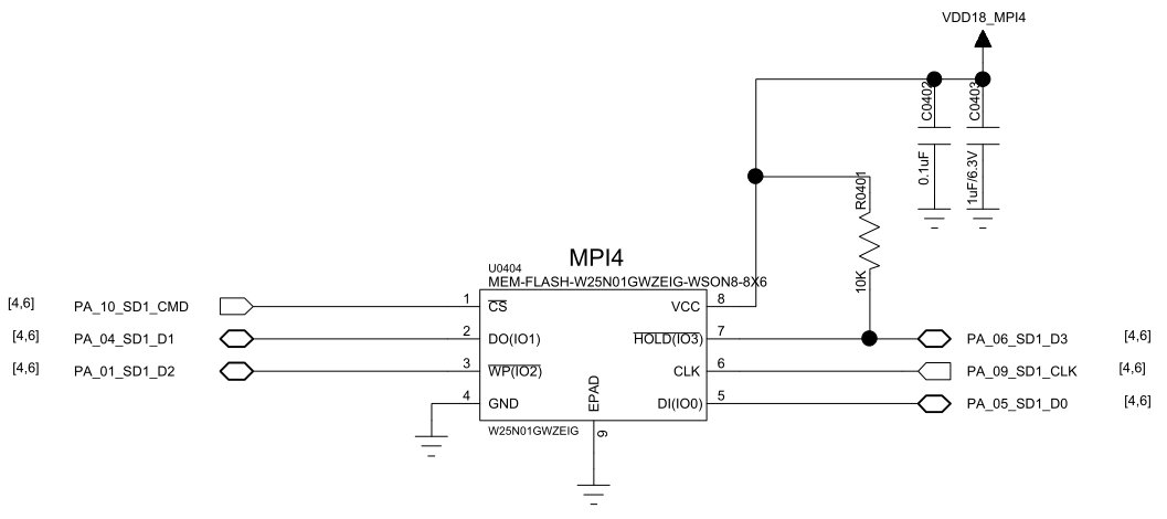
| Flash Signal | I/O Signal (MPI4) | Description |
|---|---|---|
| CS# | PA10 | Chip select, active low |
| SO | PA04 | Data Input (Data Input Output 1) |
| WP# | PA01 | Write Protect Output (Data Input Output 2) |
| SI | PA05 | Data Output (Data Input Output 0) |
| SCLK | PA09 | Serial Clock Output |
| Hold# | PA06 | Data Output (Data Input Output 3) |
Notes
- If the production line needs to flash firmware to the external Flash, the download-tool software must drive the external Flash's power-control pin PA43 high to enable its power.
- The SPI NAND Flash's Hold# pin must be pulled up to the SPI NAND Flash supply through a 10 kΩ resistor.
5.5.2.2. SDIO eMMC/Micro SD Interface
The SF32LB58x series supports 2 SDIO interfaces. On the EVB, SD1 connects to eMMC or SD NAND by default, and SD2 connects to an SD card or Wi-Fi chip.
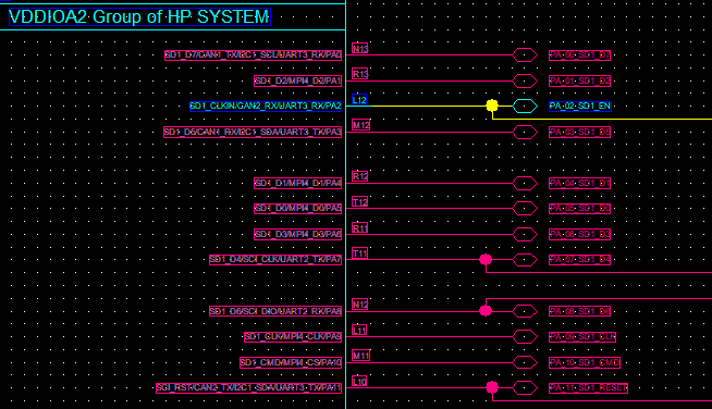
SD1 uses 12 GPIOs (PA00-PA11) powered from the VDDIOA2 domain, supporting 1.8 V or 3.3 V, selectable according to the peripheral's interface level. SPI NAND Flash and eMMC are recommended at 1.8 V; SD NAND Flash dies only support 3.3 V interface levels, so VDDIOA2 must be set to 3.3 V in that case.
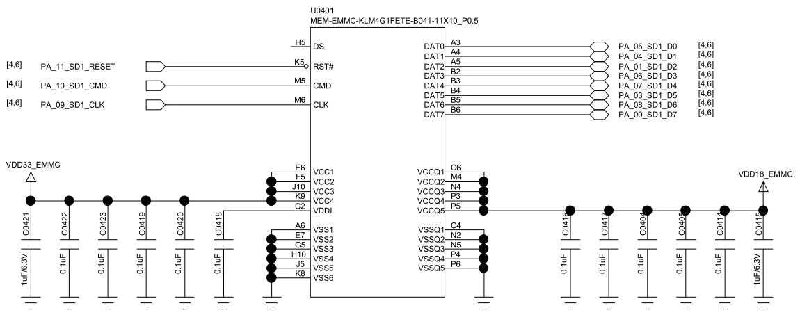
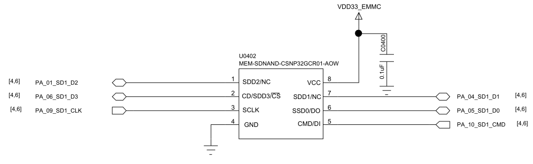
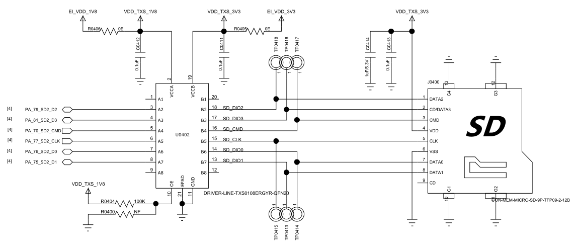
| SD1 Signal | I/O Signal | Description |
|---|---|---|
| SD1_D7 | PA00 | Data 7 |
| SD1_D2 | PA01 | Data 6 |
| SD1_D5 | PA03 | Data 5 |
| SD1_D1 | PA04 | Data 1 |
| SD1_D0 | PA05 | Data 0 |
| SD1_D3 | PA06 | Data 3 |
| SD1_D4 | PA07 | Data 4 |
| SD1_D6 | PA08 | Data 6 |
| SD1_CLK | PA09 | Clock signal |
| SD1_CMD | PA10 | Command signal |
SD1 label check
Some SF32LB58x application-note tables label both SD1_D2 and SD1_D6 as "Data 6," while SD1_D7 is labeled "Data 7." Treat the SD1 pin definitions in the chip datasheet as authoritative before release.
| SD2 Signal | I/O Signal | Description |
|---|---|---|
| SD2_CMD | PA70 | Command signal |
| SD2_D1 | PA75 | Data 1 |
| SD2_D0 | PA76 | Data 0 |
| SD2_CLK | PA77 | Clock signal |
| SD2_D2 | PA79 | Data 2 |
| SD2_D3 | PA81 | Data 3 |
5.5.3. USB
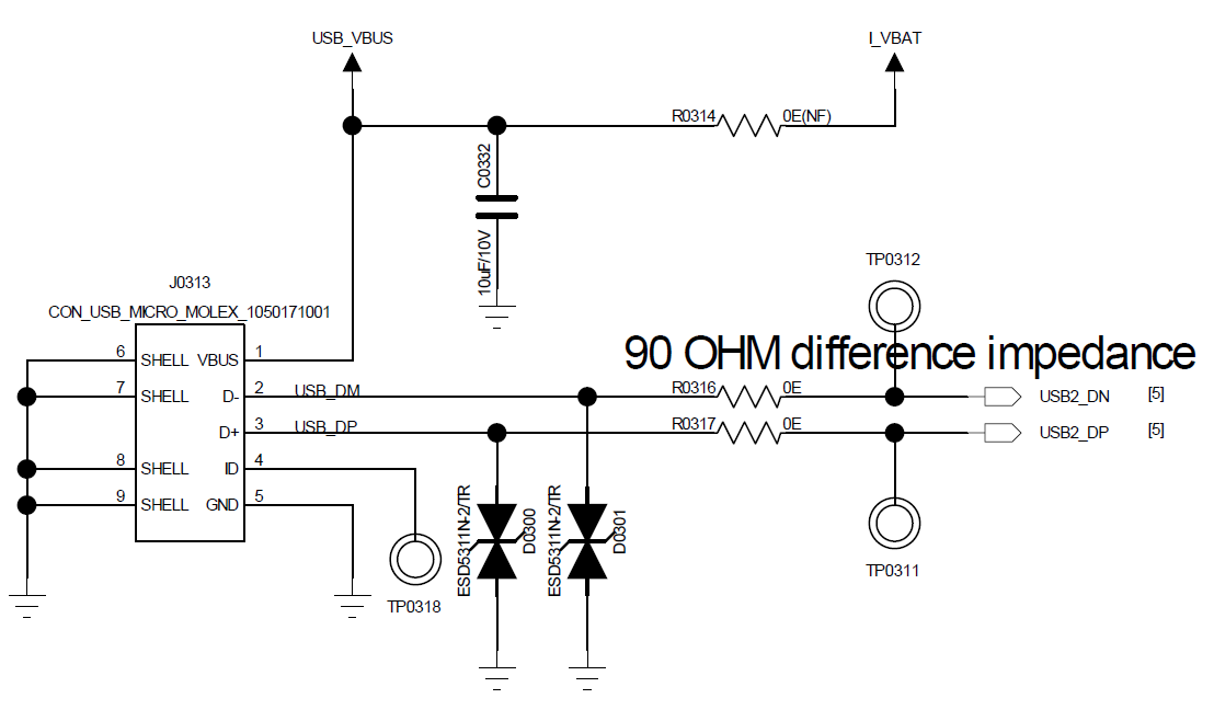
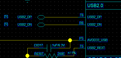
The SF32LB58x series USB supports USB2.0 HS in both Host and Device modes. A TVS diode must be connected across USB DP and DM to ground, with junction capacitance below 5 pF; DP/DM PCB traces should be controlled to 90 Ω differential impedance.
5.6. Manufacturing
5.6.1. Debug and Download Interface
The SF32LB58x series supports the Arm®-standard SWD debug interface for connection to EDA tools for single-step debugging. When connecting a SEGGER® J-Link® probe, its power source must be reconfigured for external supply, powered from the SF32LB58x board itself.
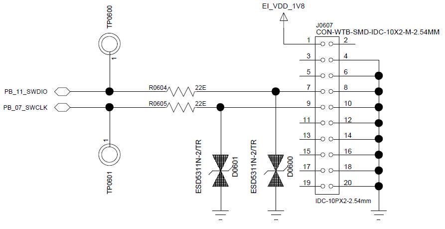
The SF32LB58x offers 1 SWD interface plus 6 selectable UART interfaces for debug output.
| UART Signal | I/O | Description |
|---|---|---|
| TXD1 | PA31 | UART1 RXD, HCPU default print port |
| RXD1 | PA32 | UART1 TXD, HCPU default print port |
| TXD2 | PA28 | UART2 RXD |
| RXD2 | PA29 | UART2 TXD |
| TXD3 | PA21 | UART3 RXD |
| RXD3 | PA20 | UART3 TXD |
| TXD4 | PB37 | UART4 RXD, LCPU default print port |
| RXD4 | PB36 | UART4 TXD, LCPU default print port |
| TXD5 | PB18 | UART5 RXD |
| RXD5 | PB17 | UART5 TXD |
| TXD6 | PB14 | UART6 RXD |
| RXD6 | PB13 | UART6 TXD |
| SWCLK | PB07 | J-Link clock signal |
| SWDIO | PB11 | J-Link data signal |
Note
UARTx RXD signals must not float; enable an internal pull-up during software initialization.
5.6.2. Production Flashing and Hardware Access
Production flashing, recovery, and calibration access should be planned before enclosure and fixture freeze. At minimum, preserve access to power, ground, SWD, required UART debug outputs, boot/configuration pins, and any board-level reset or PMIC control points needed to recover a non-booting image.
5.6.3. Schematic and PCB Drawing Checklists
- The power scheme (integrated PMU direct supply, or paired with SF30147C) matches the system power budget
- The Mode boot-configuration pin has an external 10 kΩ resistor and a reserved test point on production boards
- The 48 MHz/32.768 kHz crystal specifications match the recommendations, with layer-2 GND removed beneath the crystal
- Storage interface selection (MPI4/SD1/SD2) matches the boot configuration, and the PA43 external Flash power-control pin is confirmed
- Display interface selection (MIPI-DSI/SPI-QSPI/MCU8080/DPI/JDI) matches the LCDC1/LCDC2 pin assignment
- Debug port (SWD + 6x UART) pins are assigned as needed, with UART RXD internal pull-up enabled
- Audio interface I2S/PDM and analog-audio multiplexing has been verified, with differential-trace budget satisfied
- USB DP/DM has a parallel TVS with junction capacitance < 5 pF
6. PCB Layout Guidelines
6.1. Package Footprint Design
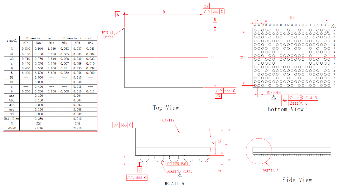
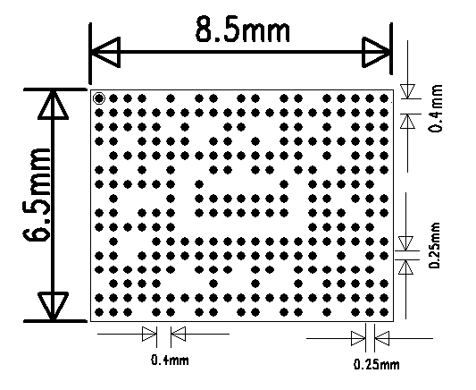
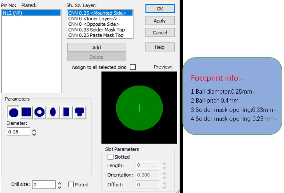
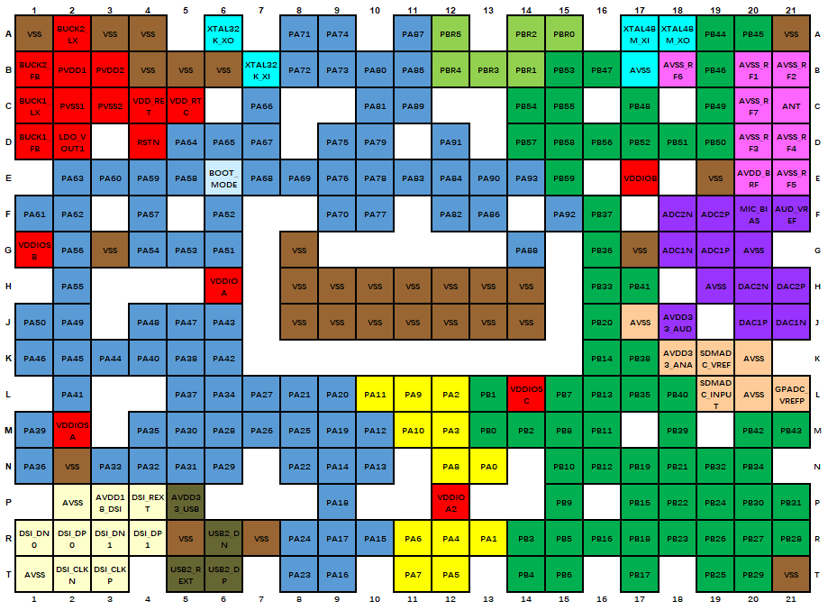
The SF32LB58x series uses a BGA256 package, 8.5 mm x 6.5 mm x 0.94 mm, 0.4 mm pitch. Refer to the official Datasheet for full package qualification data.
6.2. PCB Stack-Up
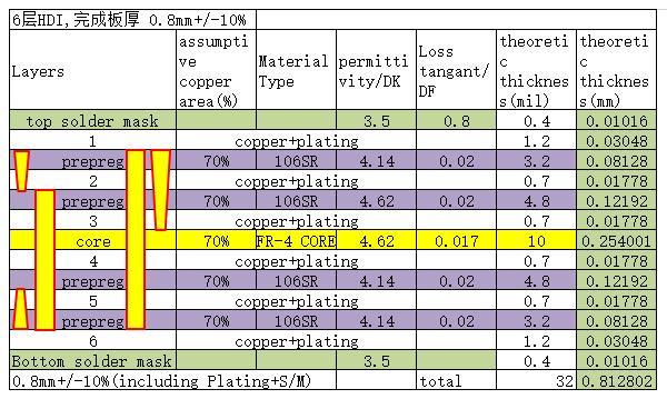
The SF32LB58x series layout supports single- or double-sided assembly. The PCB must be an HDI board — PTH is not supported; a 6HDI-2 stack-up is recommended.
6.3. General PCB Design Rules
Refer to the general PCB design-rule figure in the official Datasheet (dimensions in mm).
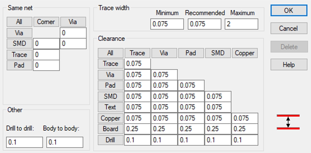
6.3.1. Blind Via Design
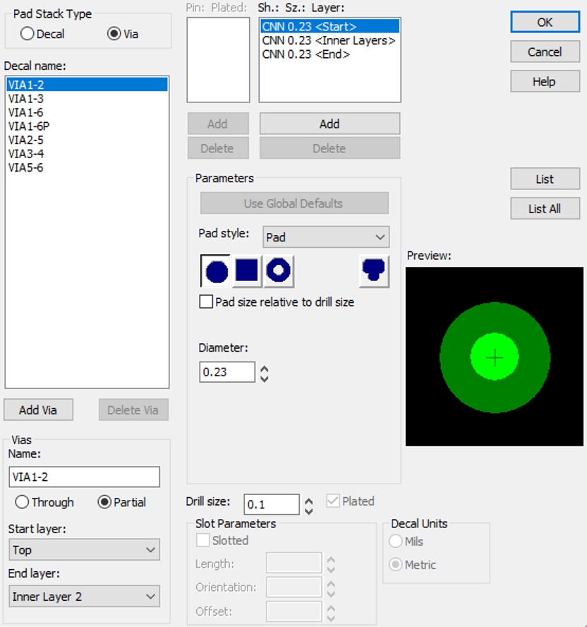
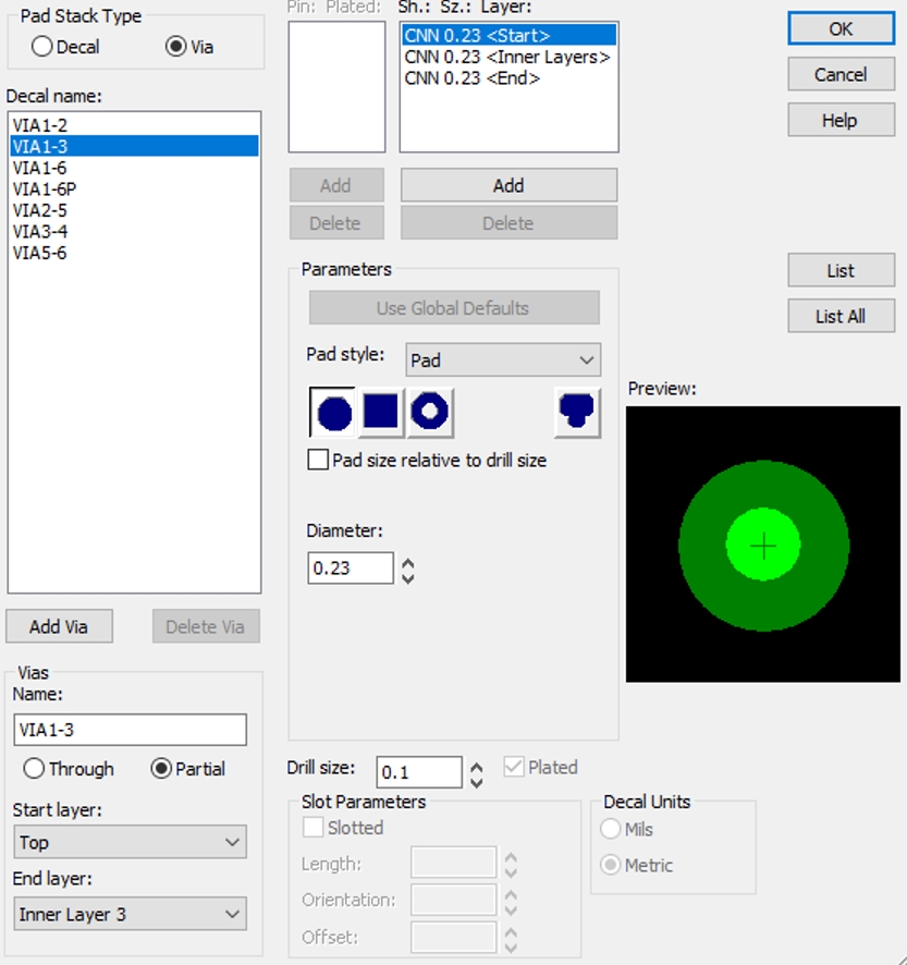
Refer to the blind-via design figures (layers 1-2 and 1-3) in the official Datasheet (dimensions in mm).
6.3.2. Buried Via Design
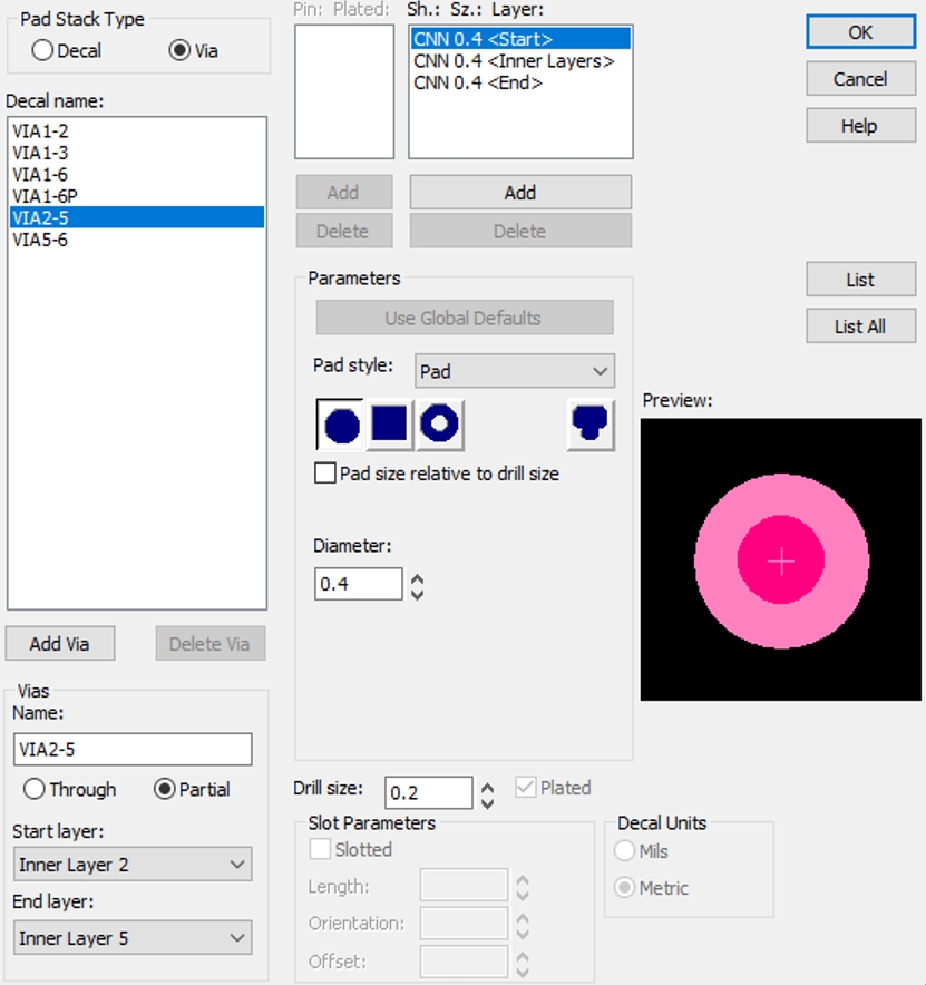
Refer to the buried-via design figure (layers 2-5) in the official Datasheet (dimensions in mm).
6.4. Trace Fanout
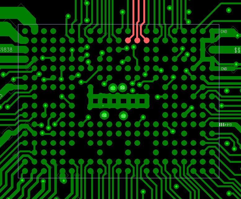
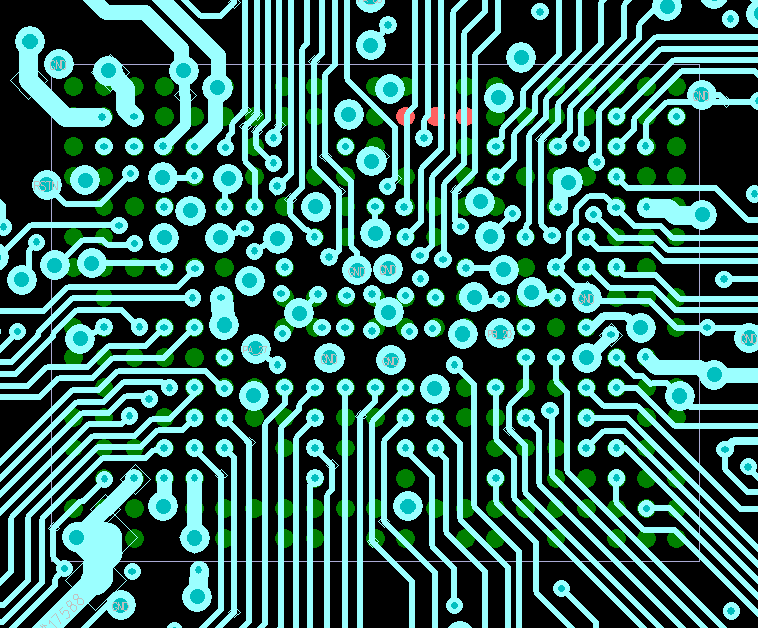
The first two rows of BGA balls are fanned out on the top layer; the remaining balls are fanned out through vias to inner layers.
6.5. Clock Interface Routing
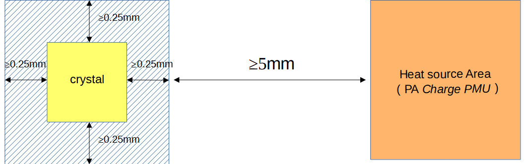
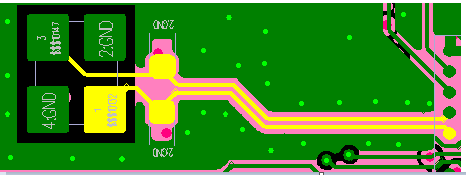
Place the crystal inside a shield can, more than 1 mm from the PCB board edge, and as far as possible from heat-generating components (such as PA, charging, and PMU circuitry) — ideally more than 5 mm away — to avoid affecting crystal frequency offset. Keep the crystal keep-out zone at least 0.25 mm from other metal or components.
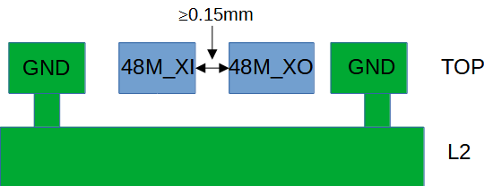
Route the 48 MHz crystal on the top layer with a length of 3-10 mm, trace width 0.075 mm, with full 3D shielding, and route away from VBAT, DC/DC, and high-speed signal lines. Keep the top layer and adjacent layer beneath the 48 MHz crystal area clear of any other routing.
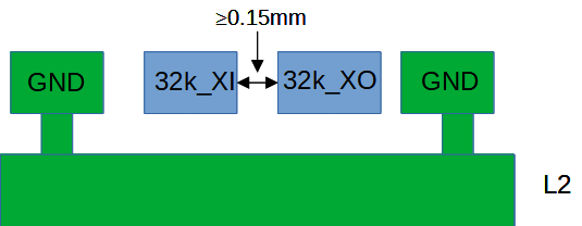
Route the 32.768 kHz crystal on the top layer with a length ≤10 mm, trace width 0.075 mm, and 32K_XI/32K_XO parallel-trace spacing ≥0.15 mm, with full 3D shielding. Keep the top layer and adjacent layer beneath the crystal area clear of any other routing.
6.6. RF Interface Routing
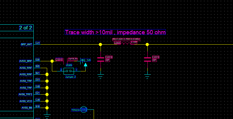
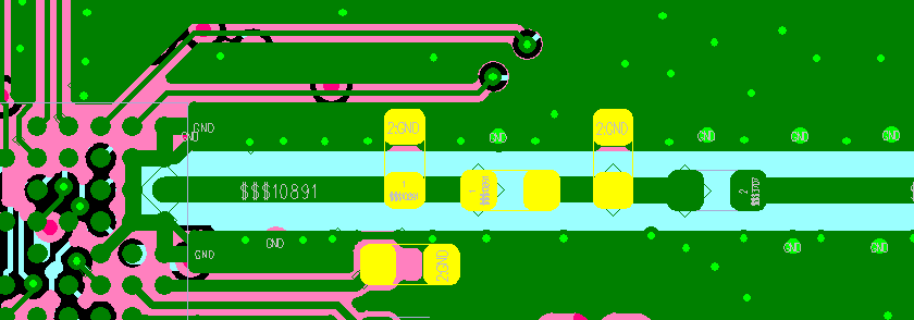
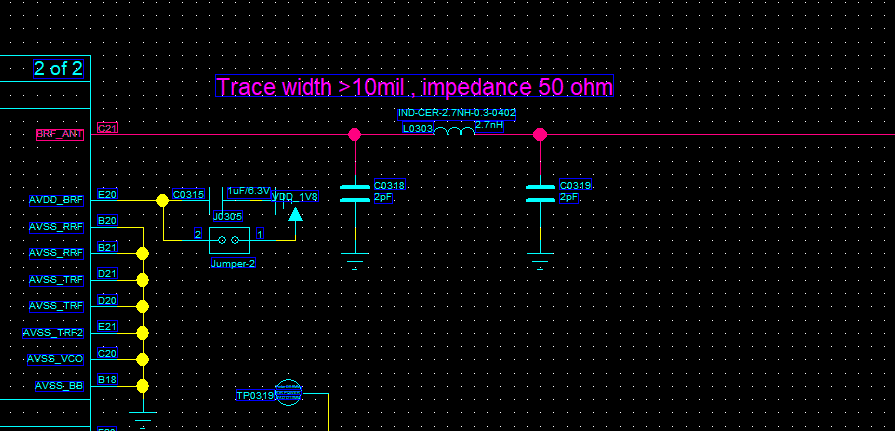
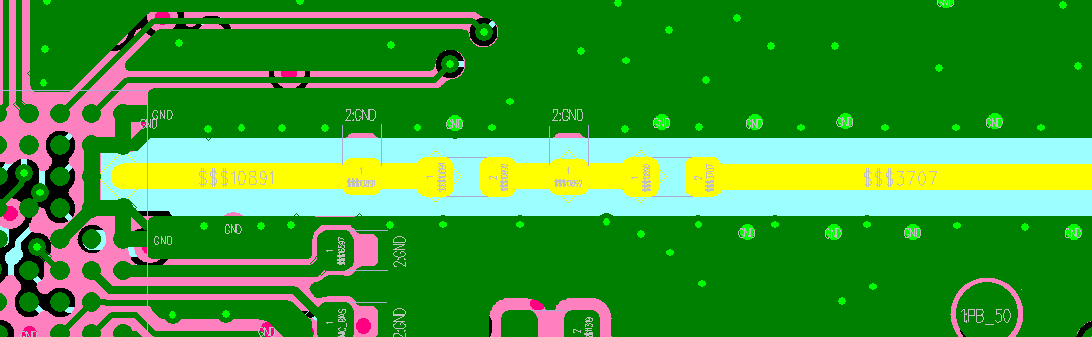
Place the RF matching circuit as close to the chip as possible, not near the antenna end. Place the AVDD_BRF RF power decoupling capacitor as close to the chip pin as possible, with its ground pin vias landing directly on the main ground plane.
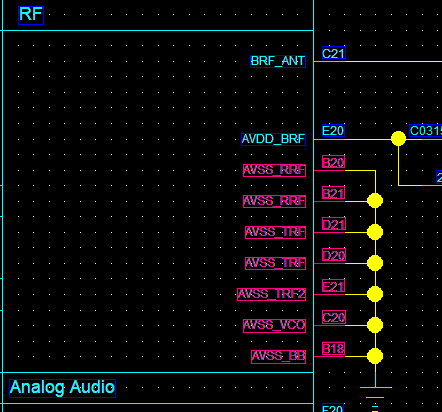
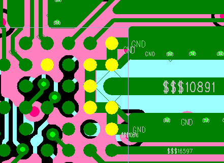
Route RF traces on the top layer where possible to avoid vias that would degrade RF performance; use a trace width greater than 10 mil, apply full 3D shielding, and avoid sharp or right angles. Add extra shielding ground vias along both sides of the RF trace, and control the RF trace to 50 Ω impedance. Keep DC-DC, VBAT, and high-speed digital signals (such as the crystal, high-frequency clocks, and I2C/SPI/SDIO/I2S/UART interface signals) out of the RF routing area. AVSS_RRF, AVSS_TRF, AVSS_TRF2, AVSS_VCO, and AVSS_BB are RF circuit ground pins that must be well grounded — place blind vias directly on their pads connecting to the main ground.
6.7. Audio Interface Routing
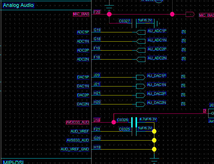
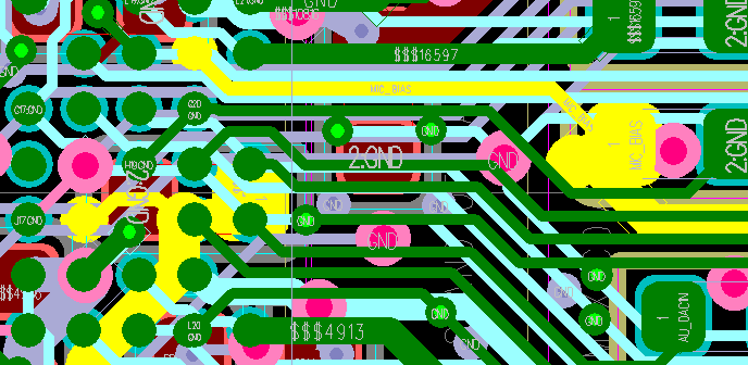
Place the AVDD33_AUD audio-supply decoupling capacitor close to its pin, with its ground pin well connected to the main ground. Place the MIC_BIAS microphone-supply decoupling capacitor close to its pin, similarly well grounded. Place the AUD_VREF decoupling capacitor close to its pin.
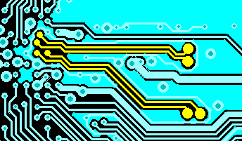
AU_ADC1P/AU_ADC1N and AU_ADC2P/AU_ADC2N are the two analog input pairs — place associated components as close to their pins as possible, route each P/N pair as a differential line with as short a trace length as possible, apply 3D shielding to the differential pair, and keep other strongly interfering signals away from these traces.
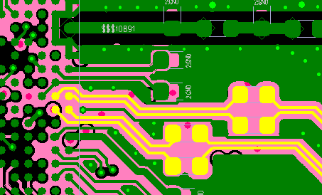
AU_DAC1P/AU_DAC1N and AU_DAC2P/AU_DAC2N are the two analog output pairs — place associated components as close to their pins as possible, route each P/N pair as a differential line as short as possible and under 2 mm, with trace parasitic capacitance below 10 pF and a differential trace width of 0.075 mm. Apply 3D shielding to the differential pair, and keep other strongly interfering signals away from these traces.
6.8. USB Interface Routing
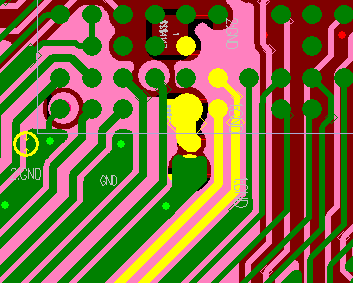
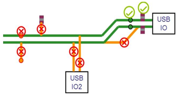
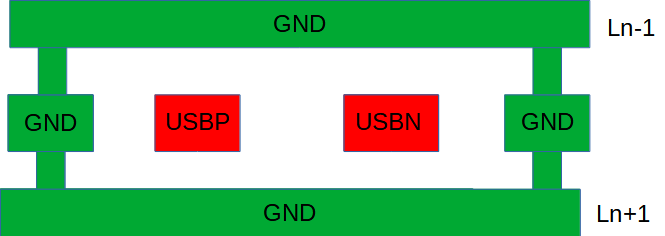
Place the AVDD33_USB decoupling capacitor close to its pin, and place the USB2_REXT calibration resistor close to its pin. USB traces must pass through the ESD-protection component pins before reaching the chip, with the ESD device's ground pin well connected to the main ground. Route USB DP/DN as a differential pair controlled to 90 Ω differential impedance, with 3D shielding applied.
6.9. SDIO Interface Routing
The SF32LB58x provides 2 SDIO interfaces, SDIO1 and SDIO2. Route all signals of each SDIO interface together rather than splitting them — total trace length ≤50 mm, with intra-group length control ≤6 mm. Apply 3D shielding to the SDIO clock signal, and shield the DATA and CMD signals as well.

6.10. DSI Interface Routing
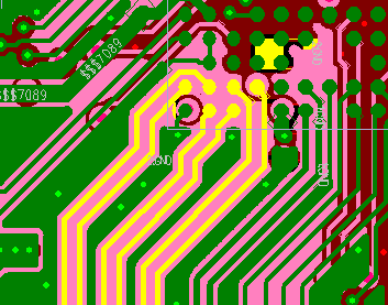
Place the AVDD18_DSI decoupling capacitor close to its pin, and place the DSI_REXT calibration resistor close to its pin. Route DSI signals as differential pairs controlled to 100 Ω differential impedance, with clock and data length-matched: intra-pair skew ≤0.5 mm and inter-pair skew ≤2 mm. Apply 3D shielding to each differential pair.
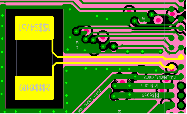
6.11. DC-DC Circuit Routing
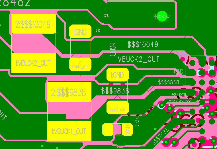
Place the DC-DC power inductor and decoupling capacitors close to the chip pins. Keep BUCK_LX traces as short and wide as possible to minimize loop inductance in the DC-DC circuit. Add extra ground vias on all DC-DC output decoupling-capacitor ground pins connecting to the main ground plane. The BUCK_FB feedback trace must not be too thin — keep it above 0.25 mm. Prohibit copper pour on the top layer beneath the power inductor, keep the adjacent layer as a complete reference ground, and avoid routing other traces through the inductor area.
6.12. Power Supply Routing
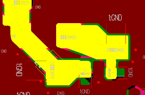
PVDD1 and PVDD2 are the power inputs to the built-in PMU module — place their decoupling capacitors close to the pins and keep the traces as wide as possible, never below 0.5 mm. PVSS1 and PVSS2 are PMU module ground pins that must be connected to the main ground through vias — avoid leaving them floating, which would affect overall PMU performance.
6.13. LDO and IO Power Input Routing
Place decoupling capacitors for all LDO outputs and IO power inputs close to their respective pins, with trace widths meeting the input current requirement — keep traces as short and wide as possible to reduce power-rail ripple and improve system stability.
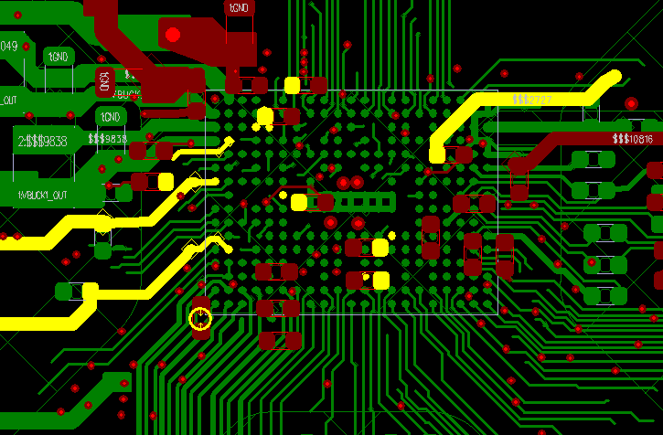
6.14. Other Interface Routing
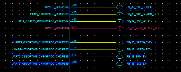
GPADC pin signal nets require full 3D shielding and must be kept away from other interference sources, such as battery-level sensing and temperature-sensing circuits.
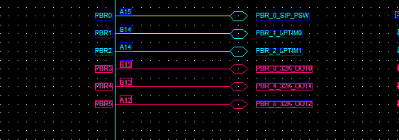
Clock input/output pin signal nets, such as the 32 kHz output, likewise require full 3D shielding and must be kept away from other interference sources.
6.15. Chip Ground Routing
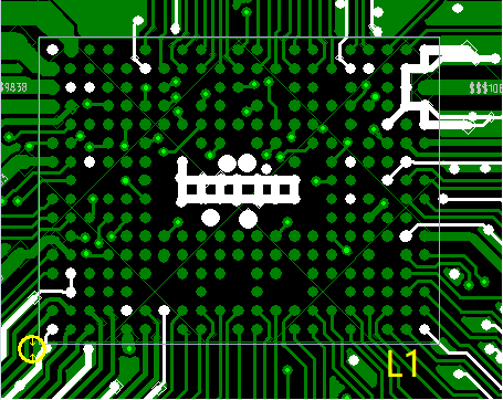
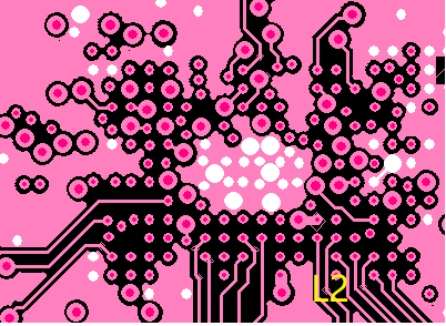
The ground network under the SF32LB58x chip's central area must be fully connected by traces, ensuring an adequate ground plane connected to the main ground plane through blind/buried vias.


6.16. EMI & ESD
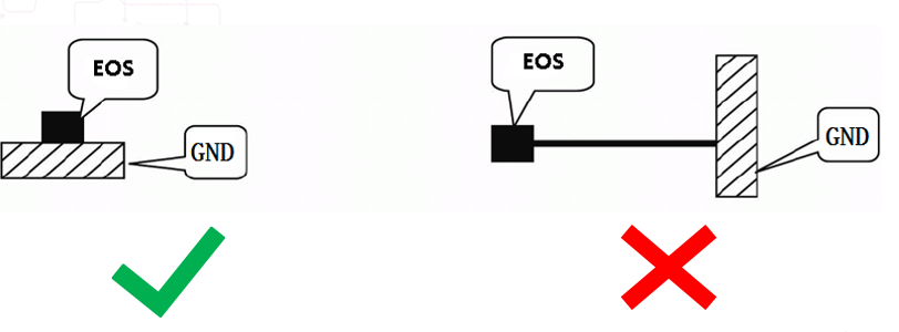
Avoid long top-layer traces outside the shield can, especially for clock and power interference sources — route them on inner layers where possible. Place ESD protection devices close to the connector pins, routing signals through the ESD device before anything else to avoid signal branching. Ensure ESD device ground pins connect to the main ground through vias, with short and wide ground pad traces to reduce impedance and improve ESD performance.
6.17. Other Considerations
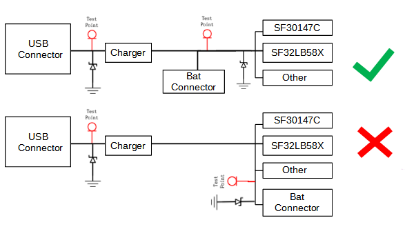
Place USB charging-line test points before the TVS diode, and place the battery-holder TVS diode before the platform connection — route so the signal always passes through the TVS before reaching the chip. Keep TVS ground-pin traces as short as possible.
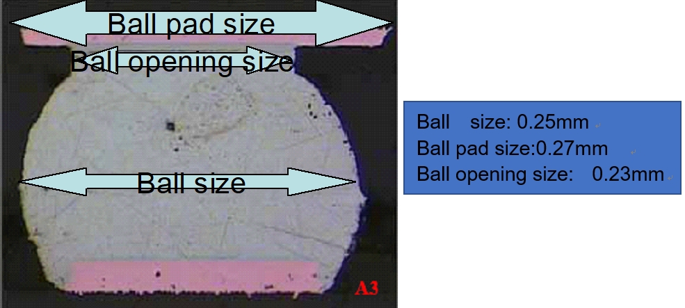
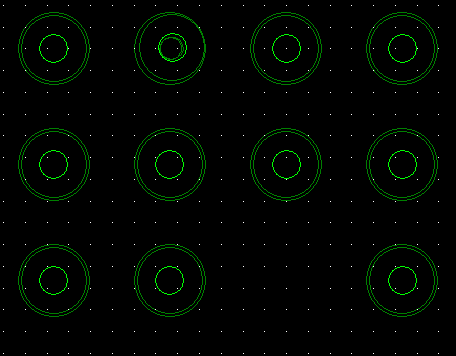
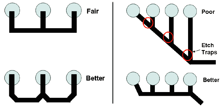
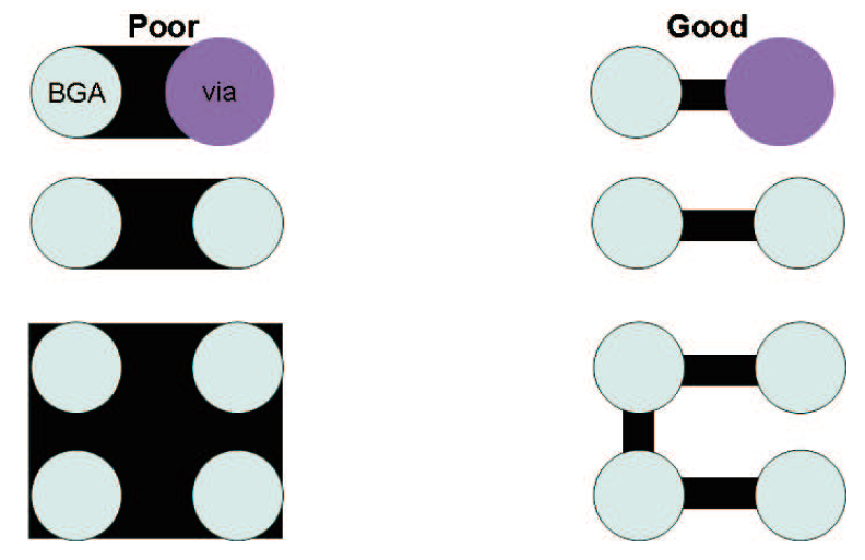
To keep solder mask off the pads and preserve solder-joint reliability, vias in BGA pads must land at the center of the ball — avoid off-center placement. For improved manufacturability yield, refer to the BGA ball-connection reference figures.
7. Design Review Checklist
- Confirmed the co-packaged Flash/PSRAM combination of the selected model matches the product requirement
- PMU supply (PVDD1/PVDD2/BUCK/LDO) and all other power pins are within the Datasheet voltage ranges
- BUCK inductor meets 4.7 uH ± tolerance, DCR ≤ 0.4 Ω, Isat ≥ 500 mA
- 48 MHz and 32.768 kHz crystals meet the recommended specifications, with routing and keep-out zones satisfied
- RF trace is 50 Ω impedance, with the matching network placed close to the chip
- Storage boot configuration (MPI4/SD1/SD2) matches the Mode boot pin setting
- Display interface (MIPI-DSI/SPI-QSPI/MCU8080/DPI/JDI) trace impedance and length-matching requirements are satisfied (DSI 100 Ω differential, SDIO intra-group ≤6 mm)
- USB and SDIO differential trace impedance and length matching meet requirements
- SWD/6x UART debug pins and production test points are reserved
- BGA pad vias are centered, and the ground plane beneath the chip is fully connected
- Key component part numbers have been verified against the latest SiFli Approved Vendor List
- The review evidence pack includes stack-up/process capability, impedance, DRC, AVL, and focused layout screenshots
- Open schematic, layout, and manufacturing questions are closed or explicitly tracked before prototype release
8. Related Documents and References
Use the latest official documents when checking electrical limits, package data, pin multiplexing, software configuration, and component qualification.
9. Appendices
The appendices collect application and reference-design context. Use them as review aids after the main schematic and PCB rules in Sections 5 and 6 have been applied.
| Need | Start Here |
|---|---|
| Application context for a rich wearable or smart terminal | Appendix A: A Typical Smart Wearable or Smart Terminal |
| Schematic screenshots and circuit-level examples | Section 5 and the SF32LB58x hardware application note |
| PCB layout screenshots for BGA, HDI, RF, DSI, USB, SDIO, audio, and power | Section 6 and the SF32LB58x hardware application note |
Appendix A. A Typical Smart Wearable or Smart Terminal
A typical SF32LB58x wearable or smart-terminal design includes the MCU, PMIC, high-resolution display, touch controller, boot storage, external memory or eMMC, sensors, vibration motor, audio input/output, Bluetooth antenna, crystals, USB, debug access, and production test access. The BGA256 package and high-speed display/storage interfaces make HDI process selection part of the system architecture, not just a PCB-layout detail.
10. Revision History
| Version | Date | Note |
|---|---|---|
| 0.0.1 | 1/2025 | Official Draft release of SF32LB58x-HW-Application |
| 1.0 | 2026-07 | Updated SF32LB58x hardware design guide with schematic, PCB, validation, and production-review guidance |