SF32LB55x Hardware Design Guide
1. Introduction
This hardware design guide provides recommendations and reference material for products based on the SF32LB55x family of mainstream AIoT microcontrollers. It is intended for hardware engineers, PCB designers, and product developers building BLE wearables, sensor-rich battery products, health-monitoring devices, and compact connected systems.
The guide covers the complete hardware development process, including package selection, power-supply design, clock circuits, RF layout, external memory, display interfaces, wake sources, sensors, audio, debug access, PCB layout, validation, and manufacturing preparation. Following these guidelines helps reduce schematic and layout risk, preserve low-power behavior, and keep the design aligned with SF32LB55x package, power, memory, RF, and interface requirements.
This document assumes a basic understanding of embedded hardware design and schematic capture. It complements the SF32LB55x datasheet, user manual, official hardware application note, reference designs, and SiFli Approved Vendor List, which remain the authority for electrical specifications, pin multiplexing, package dimensions, component qualification, and production limits.
SiFli's chip model guide notes one important caveat: the 55x suffix naming predates the later 52/56/58 convention and does not fully follow it. For interface availability, package-dependent capability, and exact memory topology, use the exact orderable part number and package reference rather than suffix inference alone.
2. Development Resources
3. Device Overview
3.1. Architecture
SF32LB55x is a mainstream AIoT MCU family for BLE-connected, sensor-rich, low-power products. The source design guide focuses on package selection, PMU rails, boot mode, dual crystal design, RF matching, external memory, MIPI/SPI/MCU8080/JDI display options, GPADC, sensors, external Bluetooth audio, debug/flashing, and production calibration.
3.2. Variants and Packages
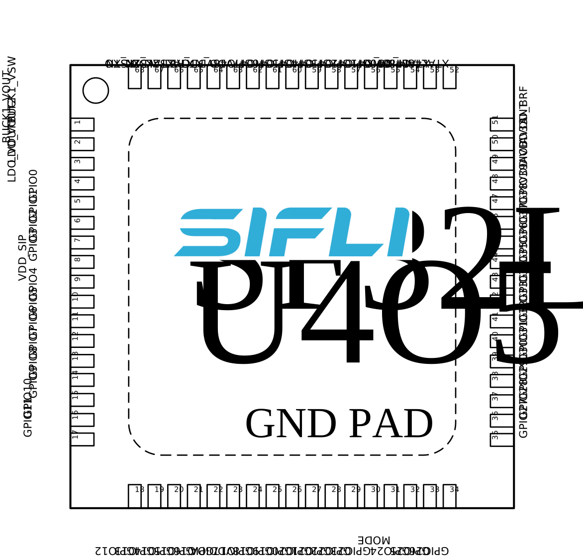
| Package Name | Size | Pin Pitch | Ball Diameter |
|---|---|---|---|
| QFN68L | 7x7x0.75 mm | 0.35 mm | - |
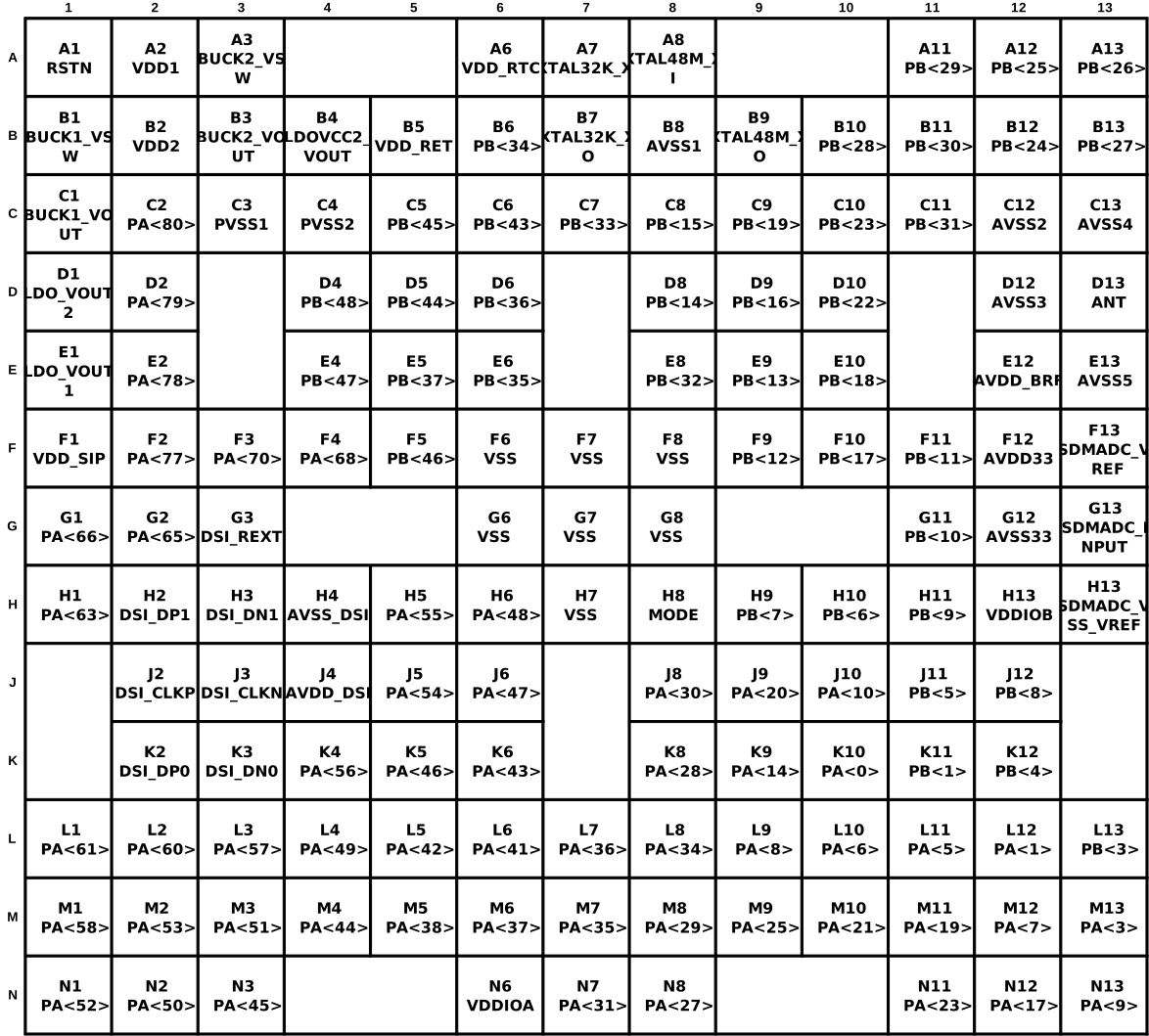
| BGA145 | 7x7x0.94 mm | 0.5 mm | 0.25 mm |
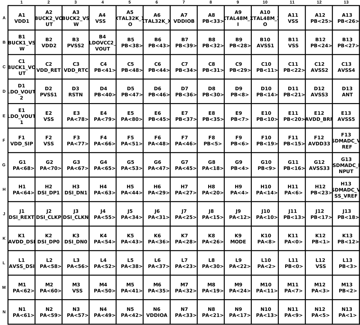
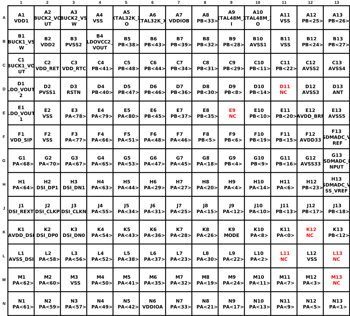
| BGA169 | 7x7x0.94 mm | 0.5 mm | 0.25 mm |
SF32LB55x supports QFN68L and multiple BGA packages. Select the package early because memory interfaces, fanout, PCB process requirements, and available GPIO differ by package.
3.3. Major Hardware Features
- QFN68L, BGA145, and BGA169 package options.
- Dual 48 MHz and 32.768 kHz crystal design requirements.
- RF matching and Bluetooth antenna layout requirements.
- OPI PSRAM, QSPI NOR/NAND Flash and PSRAM, SDIO eMMC or Micro SD interfaces.
- MIPI DSI, SPI/QSPI, MCU8080, and JDI display options.
- Wake button, vibration motor, wake interrupt, GPADC, sensor, and external Bluetooth audio design guidance.
- DBG-UART, SWD, production flashing, and crystal calibration support.
3.4. Typical Applications
SF32LB55x fits BLE wearables, fitness bands, sports and cycling computers, health-monitoring devices, sensor-rich portable products, and compact battery-powered AIoT nodes.
4. Design at a Glance
4.1. Engineering Summary
| Topic | Design Focus |
|---|---|
| Package | Choose QFN68L or BGA package before pin planning and PCB stack-up. |
| Power | Review PMU rails, other power pins, required capacitors, POR/BOR/reset, and BUCK mode. |
| Clock | Use 48 MHz and 32.768 kHz crystals that meet CL, ppm, and ESR requirements. |
| RF | Keep matching network close to the chip and preserve a clean 50 ohm antenna path. |
| Memory | Select OPI, QSPI, or SDIO storage based on package and boot strategy. |
| Display | Select MIPI DSI, SPI/QSPI, MCU8080, or JDI early because pin groups and layout differ. |
| Production | Reserve DBG-UART, SWD, boot-mode, power, and RF/crystal calibration access. |
4.2. Hardware Design Flow
- Confirm package, memory strategy, display interface, and low-power target.
- Define the power tree, PMU rails, BUCK/LDO behavior, and reset circuit.
- Select crystals, RF matching topology, and antenna layout constraints.
- Assign memory, display, wake, sensor, audio, debug, and production-test pins.
- Lock PCB stack-up, fanout, impedance, ESD, RF, and high-speed interface constraints.
- Review the Section 7 checklist before schematic freeze, layout release, and EVT.
4.3. Review Evidence Pack
Before EVT, archive the datasheet/user-manual versions, package drawing, schematic PDF, PCB stack-up, impedance report, DRC/ERC reports, power tree, boot-mode table, RF layout screenshots, crystal layout screenshots, memory/display routing screenshots, and production test-point plan.
5. Schematic Design Guidelines
| Group | Topics |
|---|---|
| Power System | PMU rails, other rails, capacitors, POR/BOR/reset, BUCK inductor. |
| Clock Generation | 48 MHz crystal, 32.768 kHz crystal, and matching-capacitor review. |
| RF | RF matching, 50-ohm antenna path, AVDD_BRF filtering, and RF keep-out. |
| Storage Interfaces | OPI PSRAM, QSPI NOR/NAND/PSRAM, and SDIO eMMC/Micro SD. |
| Display and Touch | MIPI DSI, SPI/QSPI, MCU8080, JDI, touch interrupt, reset, backlight, and panel power. |
| Wake, Analog, and Manufacturing | Wake pins, GPADC divider examples, DBG-UART, SWD, download, and calibration access. |
| User Interfaces | Wake button, vibration motor, GPADC, sensors, Bluetooth audio. |
| Manufacturing | Debug/flashing, production flashing, crystal calibration. |
5.1. Power System
| PMU Power Supply Pins | Minimum Voltage (V) | Typical Voltage (V) | Maximum Voltage (V) | Maximum Current (mA) | Detailed Description |
|---|---|---|---|---|---|
| VDD1 | 1.71 | 1.8 | 3.6 | 50 | VDD1 Power Supply input |
| VDD2 | 1.71 | 1.8 | 3.6 | 50 | VDD2 Power Supply input |
| BUCK1_VSW BUCK1_VOUT | - | 1.25 | - | 50 | BUCK1 VSW output, connected to the inductor; internal Power Supply input 1, connected to the other end of the inductor and an external capacitor |
| BUCK2_VSW BUCK2_VOUT LDOVCC2_VOUT | - | 0.9 | - | 50 | BUCK2 VSW output, connected to the inductor; internal Power Supply input 2, connected to the other end of the inductor and an external capacitor |
| LDO_VOUT1 | - | 1.1 | - | 50 | LDO output 1, connect an external capacitor |
| LDO_VOUT2 | - | 0.9 | - | 20 | LDO output 2, connect an external capacitor |
| VDD_RET | - | 0.9 | - | 1 | RET LDO output, connect an external capacitor |
| VDD_RTC | - | 1.1 | - | 1 | RTC LDO output, connect an external capacitor |
| Other Power Supply Pins | Minimum Voltage (V) | Typical Voltage (V) | Maximum Voltage (V) | Maximum Current (mA) | Detailed Description |
|---|---|---|---|---|---|
| AVDD_BRF | 1.71 | 1.8 | 3.63 | 30 | RF Power Supply input |
| AVDD_DSI | 1.71 | 1.8 | 2.75 | 20 | MIPI DSI Power Supply input; power must be supplied |
| VDD_SIP | 1.71 | 1.8 | 1.98 | 30 | Power Supply input for the co-packaged memory chip |
| AVDD33 | 3.15 | 3.3 | 3.63 | 50 | Power Supply input |
| VDDIOA | 1.71 | 1.8 | 3.63 | - | PA I/O Power Supply input |
| VDDIOB | 1.71 | 1.8 | 3.63 | - | PB I/O Power Supply input |
| Power Supply pins | Capacitor | Detailed description |
|---|---|---|
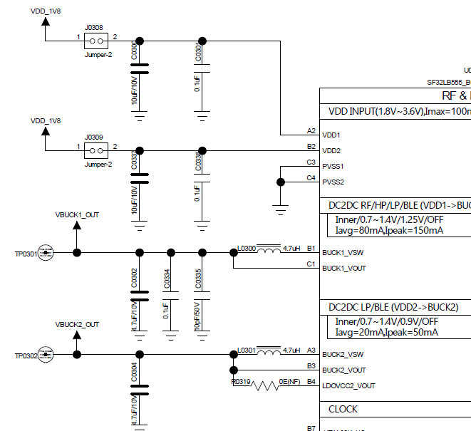
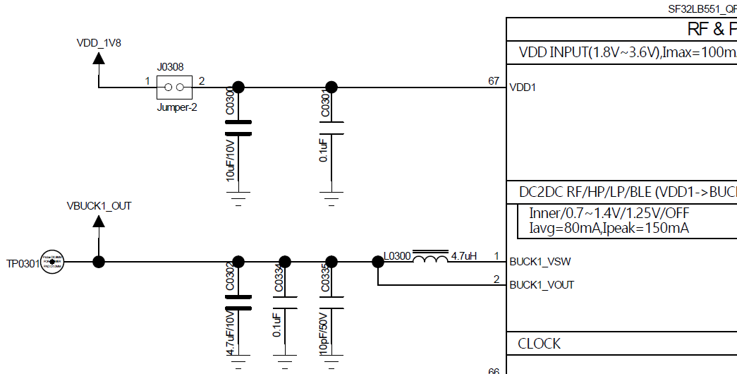
| VDD1 VDD2 | 0.1uF + 10uF | Short VDD1 and VDD2 together. Place at least two capacitors, 10uF and 0.1uF, close to the pins |
| BUCK1_VSW BUCK1_VOUT | 0.1uF + 4.7uF | Place at least two capacitors, 4.7uF and 0.1uF, close to the pins |
| BUCK2_VSW BUCK2_VOUT | 0.1uF + 4.7uF | Place at least two capacitors, 4.7uF and 0.1uF, close to the pins |
| LDOVCC2_VOUT | 0.1uF + 4.7uF | When BUCK2 is configured in BUCK mode, leave this pin floating; when BUCK2 is configured in LDO mode, leave BUCK2_VSW floating, short LDOVCC2_VOUT and BUCK2_VOUT together, and place at least two capacitors, 4.7uF and 0.1uF, close to the pins |
| LDO_VOUT1 | 4.7uF | Place at least one 4.7uF capacitor close to the pin |
| LDO_VOUT2 | 4.7uF | Place at least one 4.7uF capacitor close to the pin |
| VDD_RET | 0.47uF | Place at least one 0.47uF capacitor close to the pin |
| VDD_RTC | 1uF | Place at least one 1uF capacitor close to the pin |
| VDD_SIP | 1uF | Place at least one 1uF capacitor close to the pin |
| SDMADC_VREF | 4.7uF | Place at least one 4.7uF capacitor close to the pin |
| AVDD_DSI | 0.1uF + 10uF | Place at least two capacitors, 10uF and 0.1uF, close to the pins |
| AVDD33 | 4.7uF | Place at least one 4.7uF capacitor close to the pin |
| AVDD_BRF | 1uF | Place at least one 1uF capacitor close to the pin |
| VDDIOA VDDIOB | 2 × 0.1uF + 2 × 1uF | Place at least two capacitors, 1uF and 0.1uF, close to each pin |
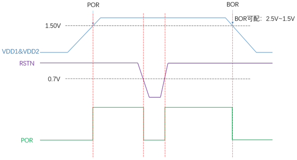
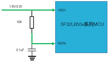
Place the required capacitors close to the corresponding pins, keep BUCK current loops compact, and verify the BUCK/LDO operating mode before layout. The reset circuit and POR/BOR timing should be checked on actual hardware.
5.2. Boot Mode
| Mode configuration | Detailed description |
|---|---|
| High | After the chip powers on and starts up, it enters download mode |
| Low | After the chip powers on and starts up, it jumps to the user program area to start |
High mode enters download mode after power-on; low mode boots the user program. Ensure production fixtures can force the required boot state and that boot-related pins are not blocked by product enclosure or test access limitations.
5.3. Clock Generation
| Crystal | Crystal specification requirements | Detailed description |
|---|---|---|
| 48MHz | 7pF≦CL≦12pF (recommended value 8.8pF) △F/F0≦±10ppm ESR≦30 ohms (recommended value 22ohms) | Crystal oscillator power consumption is related to CL and ESR. The smaller the CL and ESR, the lower the power consumption. For optimal power performance, it is recommended to use components with relatively smaller CL and ESR values within the required range. Reserve parallel matching capacitors next to the crystal. When CL<12pF, no capacitors need to be mounted |
| 32.768KHz | CL≦12.5pF (recommended value 7pF) △F/F0≦±20ppm ESR≦80k ohms (recommended value 38Kohms) | Crystal power consumption is related to CL and ESR. The smaller the CL and ESR, the lower the power consumption. For optimal power consumption performance, it is recommended to use components with relatively small CL and ESR values within the required range. Reserve parallel matching capacitors next to the crystal. When CL<12.5pF, no capacitor needs to be soldered |
Place both crystals close to the chip, keep traces short and symmetric, reserve matching capacitor footprints, and protect crystal nets from RF, BUCK, display, and motor noise.
5.4. RF
The SF32LB55x RF front end uses on-chip wideband matching-filter technology. Keep the RF PCB trace at 50 ohms characteristic impedance, reserve a π-type matching network for spurious filtering and antenna matching, and determine final component values by testing the actual antenna and PCB layout. If the selected antenna is already matched, no additional RF components are normally required beyond the reserved network.
Keep RF routing on a continuous reference ground, place the matching circuit close to the chip side, keep AVDD_BRF filtering close to the pin, and keep DC-DC, VBAT, crystal, high-speed clock, SPI, SDIO, I2S, and UART traces away from the RF area.
5.5. Storage Interfaces
SF32LB55x supports OPI PSRAM, QSPI NOR/NAND Flash and PSRAM, and SDIO eMMC or Micro SD options. Package selection affects which pins and interfaces are available, so storage selection should be completed before pin locking and PCB stack-up review.
| PSRAM signal | I/O | Detailed description |
|---|---|---|
| CS# | PA37 | Chip select output |
| CLK | PA20 | Clock output |
| DQS | PA35 | DQ strobe clock output for DQ[7:0] |
| DQ0 | PA28 | Data In/Out 0 |
| DQ1 | PA29 | Data In/Out 1 |
| DQ2 | PA30 | Data In/Out 2 |
| DQ3 | PA31 | Data In/Out 3 |
| DQ4 | PA34 | Data In/Out 4 |
| DQ5 | PA36 | Data In/Out 5 |
| DQ6 | PA38 | Data In/Out 6 |
| DQ7 | PA42 | Data In/Out 7 |
| PSRAM signal | I/O | Detailed description |
|---|---|---|
| CS# | PA07 | Chip select input |
| CLK | PA08 | Clock input |
| DQS | PA15 | DQ strobe clock input for DQ[7:0] |
| DQ0 | PA02 | Data In/Out 0 |
| DQ1 | PA04 | Data In/Out 1 |
| DQ2 | PA05 | Data In/Out 2 |
| DQ3 | PA06 | Data In/Out 3 |
| DQ4 | PA09 | Data In/Out 4 |
| DQ5 | PA11 | Data In/Out 5 |
| DQ6 | PA12 | Data In/Out 6 |
| DQ7 | PA13 | Data In/Out 7 |
| PSRAM signal | I/O | Detailed description |
|---|---|---|
| CS# | PA07 | Chip select input |
| CLK | PA08 | Clock input |
| DQS | PA26 | DQ strobe clock input for DQ[7:0] |
| DQ0 | PA18 | Data In/Out 0 |
| DQ1 | PA22 | Data In/Out 1 |
| DQ2 | PA24 | Data In/Out 2 |
| DQ3 | PA32 | Data In/Out 3 |
| DQ4 | PA33 | Data In/Out 4 |
| DQ5 | PA59 | Data In/Out 5 |
| DQ6 | PA62 | Data In/Out 6 |
| DQ7 | PA64 | Data In/Out 7 |
| Flash signal | QFN68 | BGA145/169 | Detailed description |
|---|---|---|---|
| CS# | GPIO9 | PA61 | Chip select, active low |
| SO | GPIO7 | PA65 | Data Input (Data Input Output 1) |
| WP# | GPIO6 | PA66 | Write Protect Output (Data Input Output 2) |
| SI | GPIO8 | PA63 | Data Output (Data Input Output 0) |
| SCLK | GPIO10 | PA60 | Serial Clock Output |
| Hold# | GPIO5 | PA68 | Data Output (Data Input Output 3) |
| Flash signal | QFN68 | BGA145/169 | Detailed description |
|---|---|---|---|
| CS# | GPIO16 | PA45 | Chip select, active low |
| SO | GPIO14 | PA49 | Data Input (Data Input Output 1) |
| WP# | GPIO13 | PA51 | Write Protect Output (Data Input Output 2) |
| SI | GPIO15 | PA47 | Data Output (Data Input Output 0) |
| SCLK | GPIO17 | PA44 | Serial Clock Output |
| Hold# | GPIO12 | PA55 | Data Output (Data Input Output 3) |
| Flash signal | QFN68 | BGA145/169 | Detailed description |
|---|---|---|---|
| CS# | - | PB33 | Chip select, active low |
| SO | - | PB36 | Data Input (Data Input Output 1) |
| WP# | - | PB37 | Write Protect Output (Data Input Output 2) |
| SI | - | PB35 | Data Output (Data Input Output 0) |
| SCLK | - | PB32 | Serial Clock Output |
| Hold# | - | PB07 | Data Output (Data Input Output 3) |
| Flash signal | QFN68 | BGA145/169 | Detailed description |
|---|---|---|---|
| CLK | GPIO10 | PA34 | Clock input |
| CMD | GPIO9 | PA36 | Command input |
| DATA0 | GPIO8 | PA28 | Data 0 |
| DATA1 | GPIO7 | PA29 | Data 1 |
| DATA2 | GPIO6 | PA30 | Data 2 |
| DATA3 | GPIO5 | PA31 | Data 3 |
| Flash signal | QFN68 | BGA145/169 | Detailed description |
|---|---|---|---|
| CLK | GPIO10 | PA34 | Clock input |
| CMD | GPIO9 | PA36 | Command input |
| DATA0 | GPIO8 | PA28 | Data 0 |
| DATA1 | GPIO7 | PA29 | Data 1 |
| DATA2 | GPIO6 | PA30 | Data 2 |
| DATA3 | GPIO5 | PA31 | Data 3 |
| DATA4 | GPIO15 | PA47 | Data 4 |
| DATA5 | GPIO14 | PA49 | Data 5 |
| DATA6 | GPIO13 | PA51 | Data 6 |
| DATA7 | GPIO12 | PA55 | Data 7 |
| Flash signal | QFN68 | BGA145/169 | Detailed description |
|---|---|---|---|
| CLK | GPIO17 | PA44 | Clock input |
| CMD | GPIO16 | PA45 | Command input |
| DATA0 | GPIO15 | PA47 | Data 0 |
| DATA1 | GPIO14 | PA49 | Data 1 |
| DATA2 | GPIO13 | PA51 | Data 2 |
| DATA3 | GPIO12 | PA55 | Data 3 |
5.6. Display and Touch Interfaces
Display choices include MIPI DSI, SPI/QSPI, MCU8080, and JDI. Choose the panel before pin assignment and PCB routing so the interface width, clocking, power control, touch interrupt, and backlight strategy are reviewed together.
| MIPI DSI signal | BGA145/169 I/O | Description |
|---|---|---|
| CLKP | DSI_CLKP | MIPI Clock signal + |
| CLKN | DSI_CLKN | MIPI Clock signal - |
| D0P | DSI_D0P | MIPI data lane 0+ |
| D0N | DSI_D0N | MIPI data lane 0- |
| D1P | DSI_D1P | MIPI data lane 1+ |
| D1N | DSI_D1N | MIPI data lane 1- |
| - | AVDD18_DSI | MIPI Power Supply input |
| - | DSI_REXT | Connect an external 10K resistor to ground |
| - | AVSS_DSI | Ground |
| TE | PA77 | Tearing effect to MCU frame signal |
| RESET | PB17 | Reset signal for the Display panel |
| SPI signal | QFN68 | BGA145/169 | Detailed description |
|---|---|---|---|
| CSX | GPIO22 | PB33 | Enable signal |
| WRX_SCL | GPIO23 | PB32 | Clock signal |
| DCX | GPIO20 | PB36 | Data/command signal in 4-wire SPI mode; data 1 in Quad-SPI mode |
| SDI_RDX | GPIO21 | PB35 | Data input signal in 3/4-wire SPI mode; data 0 in Quad-SPI mode |
| SDO | GPIO21 | PB35 | Data output signal in 3/4-wire SPI mode; short it together with SDI_RDX |
| D[0] | GPIO19 | PB37 | Data 2 in Quad-SPI mode |
| D[1] | GPIO18 | PB07 | Data 3 in Quad-SPI mode |
| REST | GPIO2 | PB17 | Reset signal for the Display panel |
| TE | GPIO3 | PB77 | Tearing effect to MCU frame signal |
| MCU8080 signal | QFN68 | BGA145/169 | Detailed description |
|---|---|---|---|
| CSX | GPIO22 | - | Chip select |
| WRX | GPIO23 | - | Writes strobe signal to write data |
| DCX | GPIO20 | - | Display data / command selection |
| RDX | GPIO21 | - | Reads strobe signal to write data |
| D[0] | GPIO19 | - | Data 0 |
| D[1] | GPIO18 | - | Data 1 |
| D[2] | GPIO17 | - | Data 2 |
| D[3] | GPIO16 | - | Data 3 |
| D[4] | GPIO15 | - | Data 4 |
| D[5] | GPIO14 | - | Data 5 |
| D[6] | GPIO13 | - | Data 6 |
| D[7] | GPIO12 | - | Data 7 |
| REST | GPIO2 | - | Reset |
| TE | GPIO3 | - | Tearing effect to MCU frame signal |
| JDI signal | I/O(LCDC1) | Detailed description |
|---|---|---|
| JDI_VCK | PA20 | Shift clock for the vertical driver |
| JDI_VST | PA31 | Start signal for the vertical driver |
| JDI_XRST | PA34 | Reset signal for the horizontal and vertical driver |
| JDI_HCK | PA36 | Shift clock for the horizontal driver |
| JDI_HST | PA38 | Start signal for the horizontal driver |
| JDI_ENB | PA42 | Write enable signal for the pixel memory |
| JDI_R1 | PA49 | Red image data (odd pixels) |
| JDI_R2 | PA51 | Red image data (even pixels) |
| JDI_G1 | PA55 | Green image data (odd pixels) |
| JDI_G2 | PA77 | Green image data (even pixels) |
| JDI_B1 | PA78 | Blue image data (odd pixels) |
| JDI_B2 | PA79 | Blue image data (even pixels) |
| JDI_XFRP | PA45 | Liquid crystal driving signal (“On” pixel) |
| JDI_VCOM/FRP | PA47 | Common electrode driving signal/ Liquid crystal driving signal (“Off” pixel) |
| JDI signal | I/O(LCDC1) | Detailed description |
|---|---|---|
| JDI_SCS | PA31 | Chip Select Signal |
| JDI_SCLK | PA20 | Serial Clock Signal |
| JDI_SO | PA34 | Serial Data Output Signal |
| JDI_DISP | PA36 | Display ON/OFF Switching Signal |
| JDI_EXTCOMIN | PA38 | COM Inversion Polarity Input |
| Touchscreen and backlight signals | QFN68 | BGA145 | BGA169 | Detailed description |
|---|---|---|---|---|
| Interrupt | GPIO1 | PA79 | PA79 | Touch status interrupt signal (wake-up capable) |
| I2C1_SCL | GPIO25 | PA10 | PA10 | Touchscreen I2C Clock signal |
| I2C1_SDA | GPIO24 | PA14 | PA14 | Touchscreen I2C data signal |
| BL_PWM | GPIO0 | - | - | Backlight PWM control signal |
| Reset | GPIO16 | PA00 | PA00 | Touch reset signal |
| Power Enable | GPIO26 | PA06 | PA03 | Touchscreen Power Supply enable signal |
5.7. Wake, GPADC, and Manufacturing Interfaces
Wake, analog, debug, and production access must be planned with the enclosure and fixture in mind. Wake pins need defined idle levels and ESD protection, GPADC dividers must balance settling time and leakage, and debug/download access must remain reachable in EVT and production.
| Interrupt Source | QFN68 | BGA145/169 | Detailed Description |
|---|---|---|---|
| WKUP_A0 | GPIO3 | PA77 | HCPU interrupt signal 0 |
| WKUP_A1 | GPIO2 | PA78 | HCPU interrupt signal 1 |
| WKUP_A2 | GPIO1 | PA79 | HCPU interrupt signal 2 |
| WKUP_A3 | GPIO0 | PA80 | HCPU interrupt signal 3 |
| WKUP_B0 | GPIO43 | PB43 | LCPU interrupt signal 0 |
| WKUP_B1 | GPIO44 | PB44 | LCPU interrupt signal 1 |
| WKUP_B2 | GPIO45 | PB45 | LCPU interrupt signal 2 |
| WKUP_B3 | GPIO46 | PB46 | LCPU interrupt signal 3 |
| WKUP_B4 | GPIO47 | PB47 | LCPU interrupt signal 4 |
| WKUP_B5 | GPIO48 | PB48 | LCPU interrupt signal 5 |
| Resistor Combination | R1(Kohm) ±%1 | R2(Kohm) ±%1 | Voltage settling time(ms) | Iq(uA) (VIN = 4.2V) |
|---|---|---|---|---|
| 1 | 1000 | 220 | 138 | 3.44 |
| 2 | 2000 | 430 | 250 | 1.73 |
| 3 | 3000 | 680 | 302 | 1.14 |
| 4 | 4300 | 910 | - | 0.81 |
| 5 | 5100 | 1100 | 420 | 0.68 |
| UART Signal | QFN68 | BGA145/169 | Detailed Description |
|---|---|---|---|
| TXD1 | GPIO13 | PA19 | UART1 RXD signal |
| RXD1 | GPIO14 | PA17 | UART1 TXD signal |
| TXD2 | - | PA07 | UART2 RXD signal |
| RXD2 | - | PA05 | UART2 TXD signal |
| TXD3 | GPIO46 | PB46 | UART3 RXD signal, system default log port |
| RXD3 | GPIO45 | PB45 | UART3 TXD signal, system default log port |
| TXD4 | - | PB14 | UART4 RXD signal |
| RXD4 | - | PB12 | UART4 TXD signal |
| TXD5 | - | PB11 | UART5 RXD signal |
| RXD5 | - | PB06 | UART5 TXD signal |
| SWCLK | GPIO41 | PB31 | SWD Clock signal |
| SWDIO | GPIO42 | PB34 | SWD data signal |
6. PCB Layout Guidelines
6.1. Footprint and Stack-Up
Use the package drawing, land-pattern requirements, and assembly capability of the selected QFN or BGA package. BGA packages require early confirmation of ball escape, via strategy, solder-mask rules, and fabrication limits.
6.2. General PCB Rules
- Keep BUCK loops short and wide, with return current close to the switching loop.
- Keep RF, crystal, GPADC, and audio regions away from switching supplies, display clocks, motors, and chargers.
- Route high-speed memory and display interfaces over continuous reference ground.
- Place ESD protection close to connectors and route signals through the protection device first.
- Provide enough test points for power, boot, debug, RF, and production calibration.
6.3. Interface Routing
Clock traces should be short, shielded, and isolated from fast digital signals. RF should be controlled as a 50 ohm path with a compact matching network. Storage and display traces should be length-controlled according to their speed and routed as grouped buses. Audio and GPADC signals should be shielded and kept away from switching currents.
7. Design Review Checklist
- Exact package, pinout, land pattern, and PCB process are confirmed.
- All PMU and auxiliary power rails match the datasheet voltage/current limits.
- Required decoupling capacitors are placed close to pins.
- POR/BOR/reset timing and boot mode are verified.
- 48 MHz and 32.768 kHz crystals meet CL, ppm, ESR, placement, and routing requirements.
- RF matching, antenna, and ground keep-out are reviewed.
- External memory and display pin groups match the selected package.
- Wake, GPADC, sensor, audio, touch, backlight, and motor circuits meet low-power requirements.
- Debug, download, production flashing, RF test, and crystal calibration access are reserved.
8. Related Documents and References
Use the latest official documents when checking electrical limits, package data, pin multiplexing, software configuration, component qualification, and manufacturing constraints.
9. Appendices
Appendix A. A Typical SF32LB55x Product
A typical SF32LB55x product includes the MCU, power tree, crystals, RF matching and antenna, external memory, display and touch controller, sensors, GPADC inputs, vibration motor, optional Bluetooth audio, debug access, and production test access. Battery-powered designs should also include low-power leakage review and fixture-access planning.
10. Revision History
| Version | Date | Notes |
|---|---|---|
| 0.1 | 2026-07 | Initial SF32LB55x hardware design guide generated from the official SiFli wiki hardware application note. |