This hardware design guide provides recommendations and reference material for products based on the SF32LB56x family of graphics-optimized AIoT microcontrollers. It is intended for hardware engineers, PCB designers, and product developers building smartwatches, connected HMI systems, medical and healthcare devices, industrial handhelds, portable instruments, and advanced e-bike or e-scooter displays.
The guide covers the complete hardware development process for both SF32LB56xU and SF32LB56xV designs, including package selection, PMIC and processor power, reset, boot mode, operating modes, crystals, RF, display, storage, audio, sensors, UART/I2C/GPTIM pin planning, PCB layout, validation, and production preparation. Following these guidelines helps reduce schematic and layout risk, protect low-power behavior, and keep U/V variant differences visible throughout the design.
This document assumes a basic understanding of embedded hardware design, schematic capture, and PCB layout. It complements the SF32LB56xU and SF32LB56xV hardware application notes, datasheets, user manuals, reference designs, and SiFli Approved Vendor List, which remain the authority for electrical specifications, pin multiplexing, package dimensions, component qualification, and production limits.
SF32LB56x targets richer display and HMI products than BLE-only sensor nodes. The official U and V hardware application notes share the same engineering themes: PMIC-based power distribution, 48 MHz and 32.768 kHz crystals, RF design, display interface selection, storage interface selection, audio, PBR pins, sensors, UART/I2C/GPTIM planning, debug/flashing, and production crystal calibration.
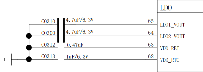
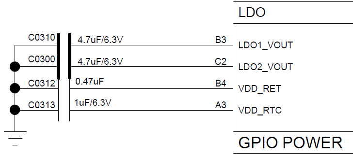
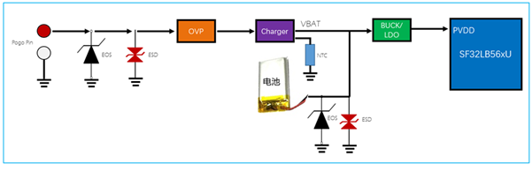
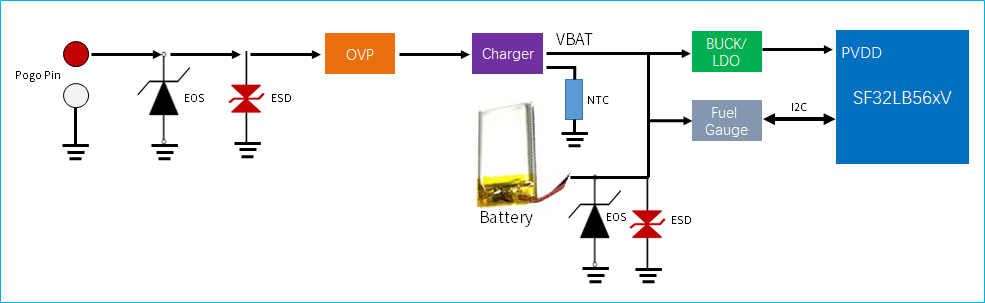
Review processor rails, required local capacitors, PMIC output assignments, reset timing, and charger wiring together. The U and V variants share the same power-design method, but their power-pin names and load assignments differ.
Table 5.1-1: SF32LB56xU Processor Power Rails
PMU Power Supply pin
Minimum Voltage(V)
Typical Voltage(V)
Maximum Voltage(V)
Maximum Current(mA)
Detailed Description
PVDD
1.7
1.8
3.6
100
PVDD Power Supply input
BUCK_LX BUCK_FB
-
1.25
-
100
BUCK_LX output, connected to the inductor; internal Power Supply input, connected to the other end of the inductor and to an external capacitor
LDO1_VOUT
-
1.1
-
50
LDO1 output, with external capacitor
LDO2_VOUT
-
0.9
-
20
LDO2 output, with external capacitor
VDD_RET
-
0.9
-
1
RET LDO output, with external capacitor
VDD_RTC
-
1.1
-
1
RTC LDO output, with external capacitor
MIC_BIAS
1.4
-
2.8
-
MIC Power Supply output
AVDD33_ANA
3.15
3.3
3.45
50
Analog Power Supply + RFPA Power Supply input
AVDD33_AUD
3.15
3.3
3.45
50
Analog audio Power Supply
VDDIO1
1.71
1.8
1.98
-
Power Supply input for the internally packaged Storage device of the big core
VDDIO2
1.71
1.8
3.45
-
Power Supply input for PA GPIO (except PA5~11)
VDDIO3
1.71
1.8
3.45
-
Power Supply input for PA5~11
VDDIO4
1.71
1.8
3.45
-
Power Supply input for PB GPIO and internally packaged Flash of the small core
GPADC_VREF
-
-
-
-
GPADC reference voltage input; connect only an external capacitor, no external power supply required
AUD_VREF
-
-
-
-
Audio reference voltage input; connect only an external capacitor, no external power supply required
Table 5.1-2: SF32LB56xV Processor Power Rails
PMU Power Supply Pin
Minimum Voltage (V)
Typical Voltage (V)
Maximum Voltage (V)
Maximum Current (mA)
Detailed Description
PVDD
1.71
1.8
3.6
100
PVDD Power Supply input
BUCK_LX BUCK_FB
-
1.25
-
100
BUCK_LX output, connected to the inductor; internal Power Supply input, connected to the other end of the inductor and to an external capacitor
LDO1_VOUT
-
1.1
-
50
LDO1 output, connected to an external capacitor
LDO2_VOUT
-
0.9
-
20
LDO2 output, connected to an external capacitor
VDD_RET
-
0.9
-
1
RET LDO output, connected to an external capacitor
VDD_RTC
-
1.1
-
1
RTC LDO output, connected to an external capacitor
MIC_BIAS
1.4
-
2.8
-
MIC Power Supply output
AVDD_BRF
1.71
1.8
3.3
1
RF Power Supply input
AVDD33_ANA
3.15
3.3
3.45
50
Analog Power Supply + RFPA Power Supply input
AVDD33_AUD
3.15
3.3
3.45
50
Analog audio Power Supply
VDDIOA
1.71
1.8
3.45
-
PA12-PA78 I/O Power Supply input
VDDIOA2
1.71
1.8
3.45
-
PA0-PA11 I/O Power Supply input
VDDIOB
1.71
1.8
3.45
-
PB I/O Power Supply input
VDDIOSA
1.71
1.8
1.98
-
SIPA Power Supply input
VDDIOSB
1.71
1.8
1.98
-
SIPB Power Supply input
VDDIOSC
1.71
1.8
1.98
-
SIPC Power Supply input
GPADC_VREF
-
-
-
-
GPADC reference voltage input; only an external capacitor is connected, no external power supply is required
AUD_VREF
-
-
-
-
Audio reference voltage input; only an external capacitor is connected, no external power supply is required
Table 5.1-3: SF32LB56xU Required Power Capacitors
Power Supply Pin
Capacitor
Detailed Description
PVDD
0.1uF + 10uF
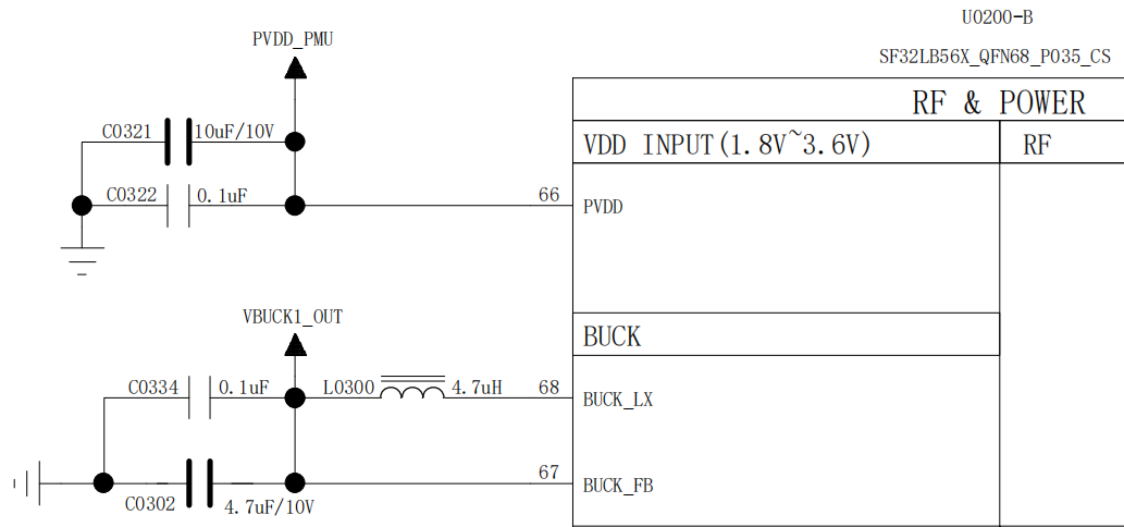
Place at least two capacitors, 10uF and 0.1uF, close to the pin.
BUCK_LX BUCK_FB
0.1uF + 4.7uF
Place at least two capacitors, 4.7uF and 0.1uF, close to the pin.
LDO1_VOUT
4.7uF
Place at least one 4.7uF capacitor close to the pin.
LDO2_VOUT
4.7uF
Place at least one 4.7uF capacitor close to the pin.
VDD_RET
0.47uF
Place at least one 0.47uF capacitor close to the pin.
VDD_RTC
1uF
Place at least one 1uF capacitor close to the pin.
AVDD33_ANA
4.7uF
Place at least one 4.7uF capacitor close to the pin.
GPADC_VREF
4.7uF
Place at least one 4.7uF capacitor close to the pin.
AVDD33_AUD
4.7uF
Place at least one 4.7uF capacitor close to the pin.
AUD_VREF
1uF
Place at least one 1uF capacitor close to the pin.
MIC_BIAS
1uF
Place at least one 1uF capacitor close to the pin.
VDDIO1
1uF
Place at least one 1uF capacitor close to the pin.
VDDIO2
1uF
Place at least one 1uF capacitor close to the pin.
VDDIO3
1uF
Place at least one 1uF capacitor close to the pin.
VDDIO4
1uF
Place at least one 1uF capacitor close to the pin.
Table 5.1-4: SF32LB56xV Required Power Capacitors
Power Supply pin
Capacitor
Detailed description
PVDD
0.1uF + 10uF
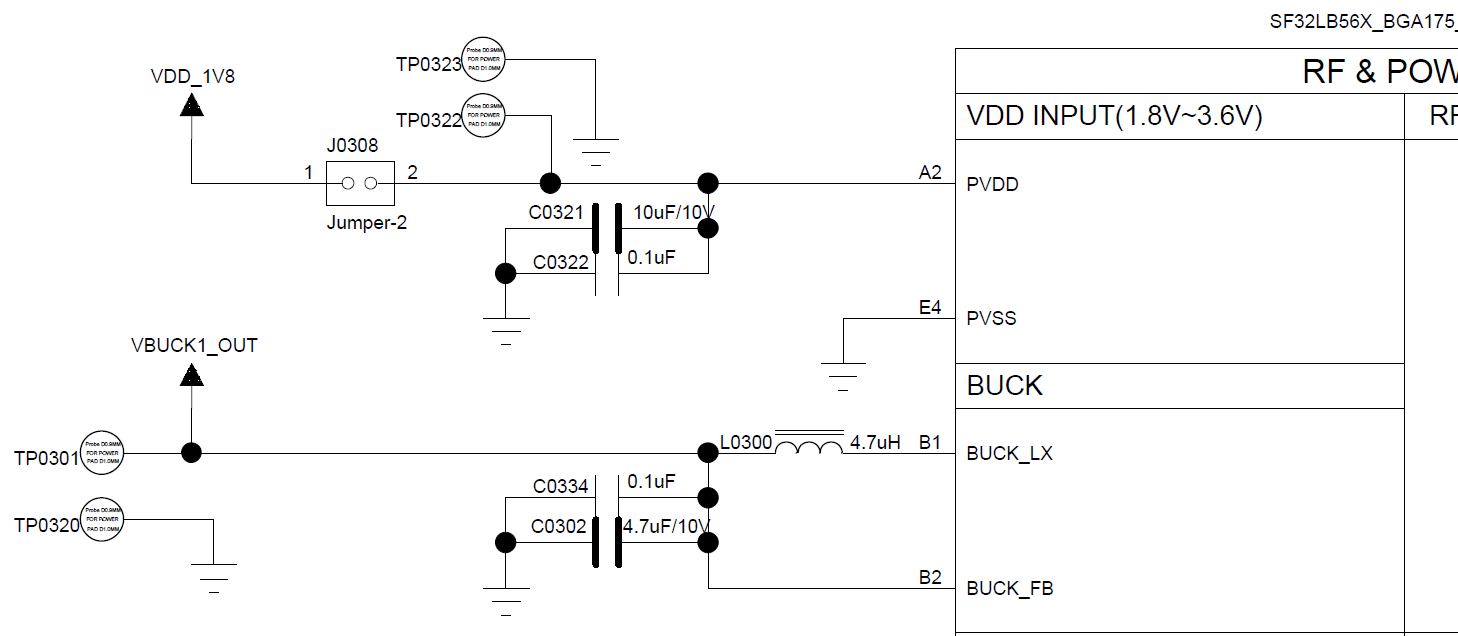
Place at least two capacitors, 10uF and 0.1uF, close to the pin.
BUCK_LX BUCK_FB
0.1uF + 4.7uF
Place at least two capacitors, 4.7uF and 0.1uF, close to the pin.
LDO1_VOUT
4.7uF
Place at least one 4.7uF capacitor close to the pin.
LDO2_VOUT
4.7uF
Place at least one 4.7uF capacitor close to the pin.
VDD_RET
0.47uF
Place at least one 0.47uF capacitor close to the pin.
VDD_RTC
1uF
Place at least one 1uF capacitor close to the pin.
AVDD_BRF
4.7uF
Place at least one 4.7uF capacitor close to the pin.
AVDD33_ANA
4.7uF
Place at least one 4.7uF capacitor close to the pin.
GPADC_VREFP
4.7uF
Place at least one 4.7uF capacitor close to the pin.
AVDD33_AUD
4.7uF
Place at least one 4.7uF capacitor close to the pin.
AUD_VREF
1uF
Place at least one 1uF capacitor close to the pin.
MIC_BIAS
1uF
Place at least one 1uF capacitor close to the pin.
VDDIOA
1uF
Place at least one 1uF capacitor close to the pin.
VDDIOA2
1uF
Place at least one 1uF capacitor close to the pin.
VDDIOB
1uF
Place at least one 1uF capacitor close to the pin.
VDDIOSA
0.1uF
Place at least one 0.1uF capacitor close to the pin.
VDDIOSB
0.1uF
Place at least one 0.1uF capacitor close to the pin.
VDDIOSC
0.1uF
Place at least one 0.1uF capacitor close to the pin.
Table 5.1-5: SF30147C PMIC Power Distribution Example for U
SF30147C Power Supply Pin
Minimum Voltage (V)
Maximum Voltage (V)
Maximum Current (mA)
Detailed Description
VBUCK
1.8
1.8
500
1.8V Power Supply inputs such as PVDD, VDDIOA, VDDIOA2, VDDIOB, VDDIOSA, VDDIOSB, VDDIOSC, AVDD_BRF of SF32LB56xU
LVSW1
1.8
1.8
100
1.8V power supply output
LVSW2
1.8
1.8
100
G-SENSOR 1.8V power supply input
LVSW3
1.8
1.8
150
Heart rate 1.8V power supply input
LVSW4
1.8
1.8
150
LCD 1.8V power supply input
LVSW5
1.8
1.8
150
1.8V power supply output
LDO1
2.8
3.3
100
3.3V Power Supply inputs such as AVDD33_ANA, AVDD33_AUD, VDDIOA2 of SF32LB56xU
LDO2
2.8
3.3
100
Motor power supply input
LDO3
2.8
3.3
100
LCD 3.3V power supply input
LDO4
2.8
3.3
100
Heart rate 3.3V power supply input
HVSW1
2.8
5
150
Analog Class-K PA power supply input
HVSW2
2.8
5
150
GPS power supply input
Table 5.1-6: SF30147C PMIC Power Distribution Example for V
SF30147C Power Supply Pin
Minimum Voltage (V)
Maximum Voltage (V)
Maximum Current (mA)
Detailed Description
VBUCK
1.8
1.8
500
1.8V Power Supply input for SF32LB56xV PVDD, VDDIOA, VDDIOA2, VDDIOB, VDDIOSA, VDDIOSB, VDDIOSC, AVDD_BRF, etc.
LVSW1
1.8
1.8
100
I2S Class-K PA logic power supply input
LVSW2
1.8
1.8
100
G-SENSOR 1.8V power supply input
LVSW3
1.8
1.8
150
Heart rate 1.8V power supply input
LVSW4
1.8
1.8
150
LCD 1.8V power supply input
LVSW5
1.8
1.8
150
EMMC CORE power supply input
LDO1
2.8
3.3
100
3.3V Power Supply input for SF32LB56xV AVDD33_ANA, AVDD33_AUD, VDDIOA2, etc.
Operating mode, wake source, pull-up rail, and leakage-current decisions should be reviewed as one topic. Use wake-capable pins for buttons, touch, sensor interrupts, charger events, and other low-power wake signals.
7pF≦CL≦12pF (recommended value 8.8pF) △F/F0≦±10ppm ESR≦30 ohms (recommended value 22ohms)
Crystal oscillator power consumption is related to CL and ESR. The smaller the CL and ESR, the lower the power consumption. For optimal power performance, it is recommended to use components with relatively smaller CL and ESR values within the required range. Reserve parallel matching capacitors next to the crystal. When CL<12pF, no capacitors need to be mounted
32.768KHz
CL≦12.5pF (recommended value 7pF) △F/F0≦±20ppm ESR≦80k ohms (recommended value 38Kohms)
Crystal power consumption is related to CL and ESR. The smaller the CL and ESR, the lower the power consumption. For optimal power consumption performance, it is recommended to use components with relatively small CL and ESR values within the required range. Reserve parallel matching capacitors next to the crystal. When CL<12.5pF, no capacitor needs to be soldered
Keep the 48 MHz and 32.768 kHz crystals close to the chip, reserve matching capacitors, and protect crystal traces from BUCK, RF, display, motor, and charger noise.
For both SF32LB56xU and SF32LB56xV designs, route the RF path as a 50-ohm controlled-impedance trace. If the selected antenna is already matched, no additional RF components are normally required, but the design should still reserve a π-type matching network for spurious filtering and final antenna tuning.
Place the RF matching network close to the chip side, not the antenna side. Keep AVDD_BRF filtering close to the chip pin, connect capacitor grounds directly to the main ground, route RF on the surface layer where practical, avoid vias and sharp corners, add dense ground shielding vias along both sides of the RF trace, and keep DC-DC, VBAT, crystal, high-speed clock, I2C, SPI, SDIO, I2S, and UART signals out of the RF area.
Display interface selection is a package-level decision. The U variant documents SPI/QSPI and JDI display options; the V variant also documents MCU8080 and DPI options. Touch interrupt, reset, and backlight controls should be assigned with wake and production access in mind.
Storage and display buses should not be assigned independently because both consume high-value GPIO groups and can drive PCB stack-up decisions. Confirm boot storage type, pull-ups, voltage domain, power-switch behavior, and fixture access before schematic freeze.
Reserve debug/flashing access, production flashing mode, crystal calibration access, power measurement points, RF test access, and PMIC control visibility. Verify the fixture can power the board, force boot/download mode, communicate with the chip, and collect calibration data.
Table 5.7-1: SF32LB56xU Debug and Flashing Interface
Signal
Pin
Detailed Description
SWCLK
PB15
JLINK Clock signal, debug interface
SWDIO
PB13
JLINK data signal, debug interface
UART4_RXD
PB16
UART receive signal, download and log printing interface
UART4_TXD
PB17
UART transmit signal, download and log printing interface
Table 5.7-2: SF32LB56xV Debug and Flashing Interface
Signal
Pin
Detailed Description
SWCLK
PB15
JLINK Clock signal, debug interface
SWDIO
PB13
JLINK data signal, debug interface
UART4_RXD
PB16
UART receive signal, download and log printing interface
UART4_TXD
PB17
UART transmit signal, download and log printing interface
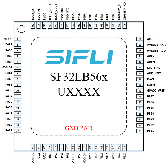
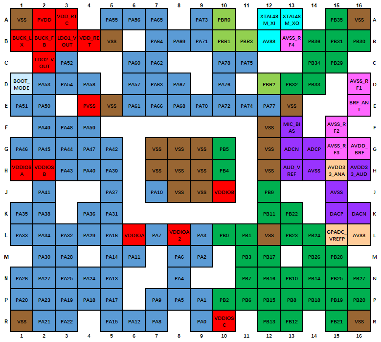
U designs must meet QFN68L footprint and fanout requirements. V designs must meet WBBGA175 footprint, solder-mask, blind-via, buried-via, and HDI process requirements. Confirm the PCB supplier can support the selected fanout strategy before layout release.
Use the latest official documents when checking electrical limits, package data, pin multiplexing, software configuration, component qualification, and manufacturing constraints.
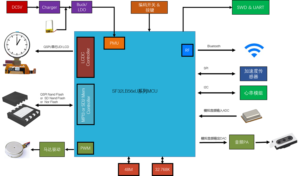
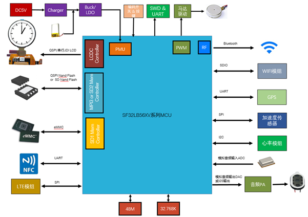
A typical SF32LB56x product includes the MCU, PMIC, display and touch controller, boot storage, optional external memory, sensors, vibration motor, audio input/output, Bluetooth antenna, crystals, debug access, and production test access. The U package favors compact QFN implementation, while the V package enables richer interfaces with BGA/HDI layout planning.