SF32LB52x Hardware Design Guide — Storage & Manufacturing
Part of the SF32LB52x Hardware Design Guide
This page covers Sections 5.6-5.7 of Schematic Design Guidelines: Storage and Connectivity, and Manufacturing. Return to RF & User Interfaces, or see the Schematic Checklist for the item-by-item review.
5.6. Storage and Connectivity
5.6.1. Storage
Quick Summary
- External boot options include SPI NOR, SPI NAND, SD NAND, and eMMC on supported regular-powered variants.
- Bootstrap pins
PA13andPA17select the boot medium. - Boot storage power switching uses
PA21; incorrect storage power behavior can block restart or increase Hibernate leakage.
Design Goal
Choose a boot medium and storage power architecture that support firmware size, update strategy, low-power states, and reliable ROM boot after reset or Hibernate.
5.6.1.1. Storage Interface Description
The chip supports external SPI NOR Flash, SPI NAND Flash, and SD NAND Flash. eMMC is supported only on the 52B/D/E/G/J regular-powered variant.
| Flash Signal | I/O Pin | Description |
|---|---|---|
| CS# | PA12 | Chip select, active low |
| SO | PA13 | Data IO1 |
| WP# | PA14 | Data IO2 / write protect |
| SI | PA15 | Data IO0 |
| SCLK | PA16 | Serial clock |
| Hold# | PA17 | Data IO3 / hold |
| SD NAND/eMMC Signal | I/O Pin | Description |
|---|---|---|
| SD2_CMD | PA15 | Command |
| SD2_D1 | PA17 | Data 1 |
| SD2_D0 | PA16 | Data 0 |
| SD2_CLK | PA14 | Clock |
| SD2_D2 | PA12 | Data 2 |
| SD2_D3 | PA13 | Data 3 |
eMMC power domains (regular-powered variant only)
eMMC chips have two power domains, VCC and VCCQ. Option 1: switch both together — lower shutdown current, but slower eMMC sleep recovery and higher average CPU power. Option 2: switch VCC only, keep VCCQ always on — higher shutdown current than option 1, but faster eMMC sleep recovery and lower average CPU power.
5.6.1.2. Boot Configuration
The chip supports booting from internal co-packaged SPI NOR Flash, external SPI NOR Flash, external SPI NAND Flash, or external SD NAND Flash (eMMC boot is not supported):
- SF32LB520Ux6 has co-packaged Flash and boots from it by default
- SF32LB523/5/7Ux6 have co-packaged PSRAM and must boot from external storage
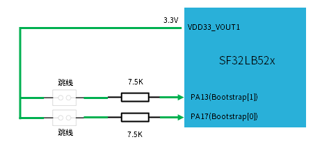
| Bootstrap[1] (PA13) | Bootstrap[0] (PA17) | Boot Medium |
|---|---|---|
| L | L | SPI NOR Flash |
| L | H | SPI NAND Flash |
| H | X | SD NAND Flash |
The chip supports booting from internal co-packaged SPI NOR Flash, external SPI NOR Flash, external SPI NAND Flash, external SD NAND Flash, or external eMMC:
- The model with co-packaged Flash (SF32LB52BU36) boots from it by default
- Models with co-packaged PSRAM (SF32LB52DUB6/EUB6/GUC6/JUD6) must boot from external storage
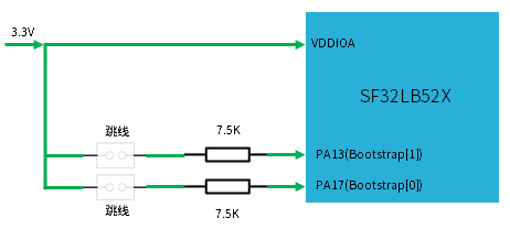
| Bootstrap[1] (PA13) | Bootstrap[0] (PA17) | Boot Medium |
|---|---|---|
| L | L | SPI NOR Flash |
| L | H | SPI NAND Flash |
| H | X | SD NAND Flash |
| H | H | eMMC |
Naming note in the original SiFli documentation
SiFli's original source document uses suffix letters "SF32LB52AUx6" and "SF32LB52D/F/HUx6" in this section, which do not match the B/D/E/G/J model naming used at the start of the same source document. This guide restates the distinction by actual co-packaged memory type (Flash vs. PSRAM); if in doubt, verify against the exact chip model and datasheet.
5.6.1.3. Boot Storage Power Control
The chip supports power-switching the boot storage medium to reduce shutdown power. The switch enable pin must be controlled through PA21, active high (on), inactive low (off).
- SF32LB520Ux6 has co-packaged Flash — power VDD18_VOUT from VDD33_VOUT1 and disable the internal VDD18_VOUT LDO
- SF32LB523/5/7Ux6 have co-packaged PSRAM — use the internal LDO; VDD18_VOUT can be externally supplied
- For external NOR Flash, power it from VDD33_VOUT1 with no extra power switch needed
- For external SPI NAND or SD NAND, power it from VDD33_VOUT1 and add a power switch
- The reference design reserves pull-up resistor footprints at PA13 and PA17 — populate based on the storage type, 7.5 kΩ recommended
- The model with co-packaged Flash (SF32LB52BU36) — add a power switch on VDD_SIP
- Models with co-packaged PSRAM (SF32LB52DUB6/EUB6/GUC6/JUD6) — if PVDD = 3.3 V and VDD_SIP uses the internal LDO, a VDD_SIP power switch is optional; if PVDD = 1.8 V, a VDD_SIP power switch is required
- External storage power is independent of VDD_SIP — add a separate power switch
- See Section 5.6.1.1 for the eMMC VCC/VCCQ power-domain tradeoffs
- All boot-related storage power switches must be controlled through PA21
- For a NOR Flash of 32 MB or larger attached via the MPI (Memory Peripheral Interface, which connects to SPI-NOR/SPI-NAND), the Flash must be power-switchable via PA21 so it exits 4-byte mode on MCU restart or Hibernate entry — otherwise ROM won't recognize the Flash. NOR Flash of 16 MB or smaller can remain always powered
- The reference design reserves pull-up resistor footprints at PA13 and PA17 — populate based on the storage type, 7.5 kΩ recommended
Common Mistakes - Storage
- Missing bootstrap resistors or populating them for the wrong boot medium.
- Leaving
PA21disconnected from the boot-storage power switch. - Treating eMMC as available on all variants.
- Keeping large NOR Flash always powered when 4-byte mode can break ROM recognition after restart.
Storage Checklist
- Boot medium is selected and documented before PCB layout.
-
PA13/PA17bootstrap pull options match the boot table. -
PA21controls all required boot-storage power switches. - eMMC VCC/VCCQ tradeoff is reviewed for regular-powered designs.
- Bring-up plan covers boot-mode strapping, storage rail timing, ID read, and firmware download.
5.6.2. Sensors
Quick Summary
- Sensors typically connect through I2C or SPI and should be power-gated when low standby current is required.
- Wake-capable sensor interrupts must be assigned before pinout freeze.
Design Goal
Keep sensor power, interrupt, and bus routing reliable while allowing unused sensors to shut down cleanly in low-power modes.
The SF32LB52x can connect to heart-rate, accelerometer, geomagnetic, and similar sensors. Choose a load switch with low Iq for sensor power switching.
Sensor Checklist
- Sensor bus, interrupt, reset, and power-enable pins are assigned.
- Sensor load switch Iq and shutdown current match the standby target.
- Pull-ups are placed on the correct sensor I/O voltage rail.
- Bring-up plan covers bus scan, interrupt wake, and sensor power cycling.
5.6.3. UART and I2C Pin Assignment
Quick Summary
- UART and I2C functions can be mapped to arbitrary PA pins.
- Pin choices should still account for boot, wake, debug, production test, and board routing constraints.
Design Goal
Use flexible pin mapping to simplify routing without blocking required boot straps, wake pins, debug access, or production fixtures.
The SF32LB52x supports UART and I2C function mapping on arbitrary PA pins.
UART/I2C Checklist
- Pull-ups, voltage domains, and bus capacitance are correct for every I2C bus.
- UART pins needed for logs, download, or external modules are accessible.
- Pin multiplexing does not conflict with bootstrap, wake, display, storage, or debug functions.
5.6.4. GPTIM Pin Assignment
Quick Summary
- GPTIM functions can be mapped to arbitrary PA pins.
- Timer outputs are commonly used for PWM, capture, motor control, backlight, or product-specific timing.
Design Goal
Reserve timer-capable functions early enough that PWM, capture, and timing features are not forced onto poor routing or wake-conflicting pins late in the design.
The SF32LB52x supports GPTIM function mapping on arbitrary PA pins.
GPTIM Checklist
- Timer channels required for PWM, capture, or control loops are listed in the pinout table.
- GPTIM pins do not conflict with backlight, motor, debug, or storage requirements.
- Bring-up plan includes checking PWM frequency, duty range, and pin polarity.
5.7. Manufacturing
5.7.1. Debug and Download Interface
Quick Summary
PA18andPA19default to DBG_UART after power-up and are multiplexed with SWD.- Reserve physical access to the debug/download pins on every prototype and production board.
Design Goal
Guarantee firmware download, debug logs, single-step debug, and failure recovery access even after the product enclosure and production fixture are defined.
The SF32LB52x supports a DBG_UART interface for download and debug, connected to a PC through a 3.3 V UART-to-USB dongle board. SWD and DBG_UART are multiplexed on PA18 and PA19; the default power-on configuration is DBG_UART, which supports single-step debugging as well as log output.
| Debug Signal | Pin | Description |
|---|---|---|
| DBG_UART_RXD | PA18 | Debug UART receive |
| DBG_UART_TXD | PA19 | Debug UART transmit |
Debug Checklist
-
PA18/PA19, ground, and the required power reference are exposed on test pads or connector pins. - Debug access remains available after enclosure, battery, and display assembly.
- UART voltage level is 3.3 V compatible with the selected adapter or fixture.
- Recovery path is documented for a board that cannot boot application firmware.
5.7.2. Production Flashing and Crystal Calibration
Quick Summary
- Production programming and crystal calibration require stable power, DBG_UART access, PA01, and the required power/ground test points.
- Fixture access should be designed before the PCB mechanical outline and enclosure are frozen.
Design Goal
Make every production board programmable, calibratable, and recoverable without manual soldering or product disassembly.
SiFli provides an offline downloader for production firmware flashing and crystal calibration. Reserve at least these test points in the hardware design: PVDD/VBAT, GND, AVDD33, DBG_UART_RXD, DBG_UART_TXD, and PA01. See the "Offline Downloader User Guide" document included in the development package for the detailed flashing and calibration process.
Production Checklist
- PVDD/VBAT, GND, AVDD33, DBG_UART_RXD, DBG_UART_TXD, and PA01 test points are reserved.
- Test pads are reachable by the intended fixture after mechanical assembly.
- Crystal calibration flow and pass/fail limits are defined with manufacturing.
- Programming, calibration, and functional-test records can be tied back to the board revision.
5.7.3. Schematic and PCB Drawing Checklists
Use the official schematic and PCB checklist published on SiFli's wiki as the formal release gate — see the Schematic Checklist for the complete, item-by-item version. The local checklists in this guide are intended to catch common engineering issues before the formal checklist review.
Release Checklist
- Schematic checklist, PCB checklist, AVL check, DRC report, and impedance report are complete.
- Evidence screenshots are archived for power, clock, RF, display, storage, audio, USB, SDIO, DC/DC, and production-test access.
- Variant-specific assumptions are documented in the review notes.
- Open hardware risks are assigned to an owner before release.