Sample with GPADC
This note consolidates the ADC guides for SF32LB52x, SF32LB55x, SF32LB56x, SF32LB57x, and SF32LB58x. The software workflow is shared, but the input limits, pad assignments, and calibration points are family-specific. Select the target family in the tables before configuring hardware or firmware.
GPADC is SiFli's general-purpose ADC for measurements such as sensors and battery voltage. It is separate from the audio ADC available on SF32LB52x, SF32LB56x, SF32LB57x, and SF32LB58x, and from the sigma-delta ADC available on SF32LB55x and SF32LB58x. This note covers GPADC only; use the target family's audio or sigma-delta documentation for those converters.
ADC Scope and Channel Model
The SF32LB52x, SF32LB55x, SF32LB56x, and SF32LB58x SDK app-note model uses eight ADC channels, GPADC_CH0 through GPADC_CH7, for analog sources such as sensor outputs and battery-voltage measurements. The SF32LB57x hardware design guide defines twelve GPADC channels: PA28–PA38 as GPADC_CH0–GPADC_CH10, plus VBAT / VBATS as GPADC_CH11. A usable voltage result depends on both the external divider network and the software calibration values.
The guide separately notes that GPADC_CH7 is the fixed battery-voltage input on SF32LB52x. On SF32LB56x, channel 7 is mapped to PB32; use the SF32LB56x mapping below rather than the SF32LB52x battery-input convention. The SF32LB57x 12-channel map and VBAT/VBATS input must also be checked separately; do not apply the eight-channel map to it.
ADC Characteristics and Input Network
| Characteristic | SF32LB55x | SF32LB52x / 56x / 58x | SF32LB57x |
|---|---|---|---|
| ADC channels | 8 | 8 | 12 |
| Battery-voltage sampling | External: route a divider into a selected GPADC input |
On-chip: SF32LB52x: GPADC_CH7 / BAT;SF32LB56x: GPADC_CH7 / PB32;SF32LB58x: GPADC_CH7 / PB39 |
On-chip:GPADC_CH11 / VBAT or VBATS |
| Sampling width | 10 bit | 12 bit | 12 bit |
| Sampling accuracy | 3–4 mV | 1–2 mV | 1–2 mV |
| Maximum sampled voltage | 1.1 V | 3.3 V | 3.3 V |
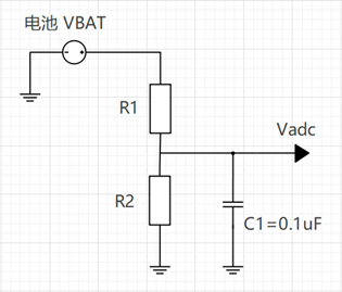
| Recommended external-divider resistors | 1000 kΩ / 220 kΩ | 470 kΩ / 1000 kΩ | 470 kΩ / 1000 kΩ |
| RC settling time | 157 ms | 200 ms | 200 ms |
Choose the divider and its RC behavior so the ADC input never exceeds the target family's documented limit. Divider tolerance affects the final measurement accuracy. The guides recommend separately calibrating the divider network on the production line to remove that error from the final result. This page treats SF32LB57x electrical characteristics as the same as SF32LB52x, SF32LB56x, and SF32LB58x, pending family-specific confirmation.
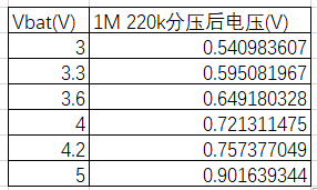
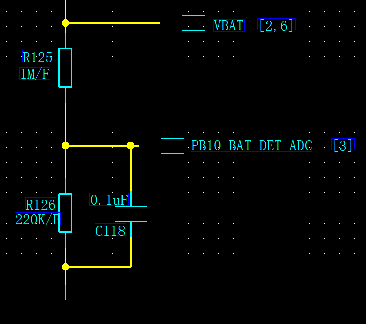
For the SF32LB55x external battery path, the upstream FAQ shows a 1 MΩ / 220 kΩ divider using 1% resistors. The high resistance reduces the divider's continuous leakage current; the 1% tolerance limits divider-ratio error and supports measurement accuracy. The divider output is the ADC test point; it is not the battery voltage itself. Use the target schematic and electrical limits when adapting this reference.
Analog Supply and Reference
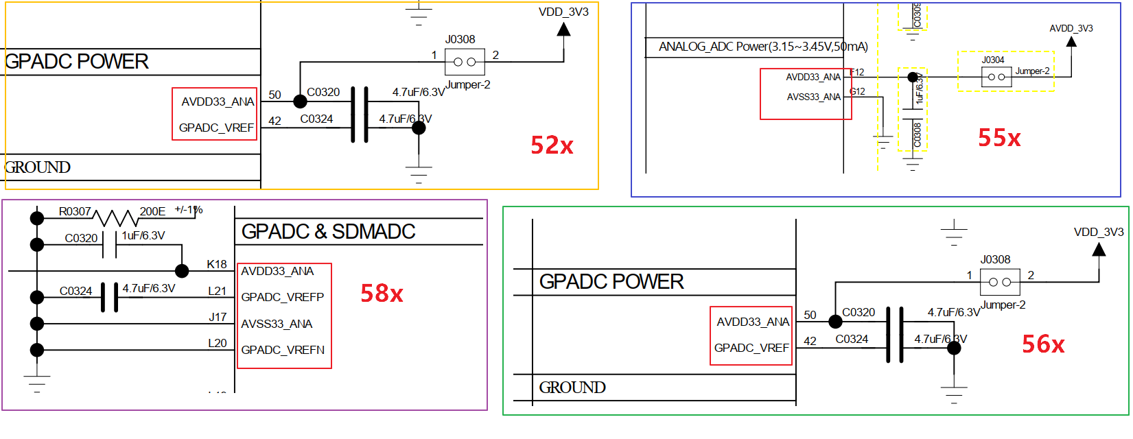
The ADC uses one analog supply domain:
AVDD33_ANAis the required, stable 3.3 V analog supply.GPADC_VREFis an internal-reference pin, not an independent supply input.
Depending on the platform, GPADC_VREF is either decoupled to ground with an external capacitor or is not brought out and uses the internal reference. Never apply a supply directly to GPADC_VREF; power the ADC through AVDD33_ANA.
Configure the ADC Pad
Set the selected input pad to its analog function before sampling. The guide's generic API examples are:
Those calls illustrate the analog-pin API, not a target-family pad selection. Select the physical input from this channel map:
| Family | GPADC_CH0 |
GPADC_CH1 |
GPADC_CH2 |
GPADC_CH3 |
GPADC_CH4 |
GPADC_CH5 |
GPADC_CH6 |
GPADC_CH7 |
|---|---|---|---|---|---|---|---|---|
| SF32LB55x | PB08 |
PB10 |
PB12 |
PB13 |
PB16 |
PB17 |
PB18 |
PB19 |
| SF32LB52x | PA28 |
PA29 |
PA30 |
PA31 |
PA32 |
PA33 |
PA34 |
BAT |
| SF32LB56x | PB22 |
PB23 |
PB24 |
PB25 |
PB26 |
PB27 |
PB28 |
PB32 |
| SF32LB58x | PB32 |
PB33 |
PB34 |
PB35 |
PB36 |
PB37 |
PB38 |
PB39 |
| SF32LB57x | PA28 |
PA29 |
PA30 |
PA31 |
PA32 |
PA33 |
PA34 |
PA35 |
SF32LB57x has four additional ADC channels: PA36 is GPADC_CH8, PA37 is GPADC_CH9, PA38 is GPADC_CH10, and VBAT / VBATS is GPADC_CH11. The VBAT / VBATS input belongs to the battery-voltage domain and has a different measurement range from normal GPADC pins. Its 12-channel map is therefore not interchangeable with the eight-channel maps above.
The SF32LB55x-only route can also assign the PIN directly to a GPADC channel, for example HAL_PIN_Set(PAD_PB08, GPADC_CH0, PIN_NOPULL, 0). Do not copy that specific assignment into a different family.

Read an ADC Channel
SiFli-SDK registers the ADC as a battery-voltage device; the guide uses bat1 as its default device name. With the RT-Thread device interface, find the device, open it read-only, enable the intended channel, and read its raw value:
uint32_t channel = 1;
uint32_t value;
rt_device_t dev = rt_device_find("bat1");

if (dev) {
    rt_device_open(dev, RT_DEVICE_FLAG_RDONLY);
    rt_device_control(dev, RT_ADC_CMD_ENABLE, (void *)channel);
    rt_device_read(dev, channel, &value, 1);
}
For HAL-level code, the guide identifies HAL_ADC_GetValue(channel) as the raw-value interface. The configured pad, selected channel, and software read must refer to the same channel.
ADC Calibration and Voltage Conversion
The guide models conversion as a linear relationship:
Offset is the raw value at 0 V; Ratio is the voltage increment per raw count. Factory calibration compensates for manufacturing variation, but the guide also describes a two-point calibration method for the assembled input path:
- Apply two accurate, stable voltages and read the corresponding ADC values.
- Use the target family's two calibration voltages rather than 0 V or the maximum input voltage.
- Use
sifli_adc_calibrationto calculate and retain the ratio and offset. - Convert later raw values with the retained calibration values, and include the divider ratio when reporting source-side voltage.
The source implementation sets ADC_RATIO_ACCURATE to 1000, with initial adc_vol_offset and adc_vol_ratio values of 200 and 3930 respectively.
SF32LB55x Calibration Ranges
The upstream OpenSiFli FAQ documents the SF32LB55x calibration flow in more detail. During sifli_adc_init, the factory-area Flash configuration identified by FACTORY_CFG_ID_ADC supplies the stored calibration readings. sifli_adc_calibration derives the linear offset and ratio from those readings; subsequent samples use the selected range's sifli_adc_get_mv calculation.
Two calibration ranges are documented:
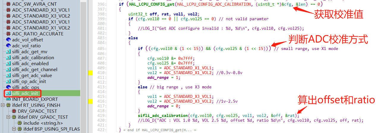
- X1 range: 0.3 V and 0.8 V. The stored calibration values have bit 15 set, so the implementation selects the small-range path. Accuracy is reduced near 0 V and above 1 V. This path disables
GPADC_ADC_CFG_REG1_ANAU_GPADC_ATTN3X, so the internal divider is off and the ADC test point must not exceed 1.1 V. - X3 range: 1.0 V and 2.5 V. This is the earlier calibration method. It enables
GPADC_ADC_CFG_REG1_ANAU_GPADC_ATTN3X, which enables the internal divider with 3× attenuation; the input must not exceed 3.3 V.

Never choose a calibration range from the table alone: use the factory configuration and target SDK implementation. The X1 and X3 behaviors are specific to the SF32LB55x material cited here, not a rule to apply to another family.
| Family | Calibration inputs |
|---|---|
| SF32LB55x | 0.3 V and 0.8 V |
| SF32LB52x / 56x / 58x | 1.0 V and 2.5 V |
| SF32LB57x | 1.0 V and 2.5 V |
static uint32_t adc_vol_offset = 200;
static uint32_t adc_vol_ratio = 3930;
#define ADC_RATIO_ACCURATE 1000

int sifli_adc_get_mv(uint32_t value)
{
    return (value - adc_vol_offset) * adc_vol_ratio / ADC_RATIO_ACCURATE;
}

int sifli_adc_calibration(uint32_t value1, uint32_t value2,
                          uint32_t vol1, uint32_t vol2,
                          uint32_t *offset, uint32_t *ratio)
{
    uint32_t gap1, gap2;

    if (offset == NULL || ratio == NULL) return 0;

    gap1 = (value1 > value2) ? (value1 - value2) : (value2 - value1);
    gap2 = (vol1 > vol2) ? (vol1 - vol2) : (vol2 - vol1);

    if (gap1 == 0) return 0;

    *ratio = gap2 * ADC_RATIO_ACCURATE / gap1;
    adc_vol_ratio = *ratio;
    *offset = value1 - (vol1 * ADC_RATIO_ACCURATE / adc_vol_ratio);
    adc_vol_offset = *offset;

    return adc_vol_offset;
}
Validate Calibration After Startup and Wake
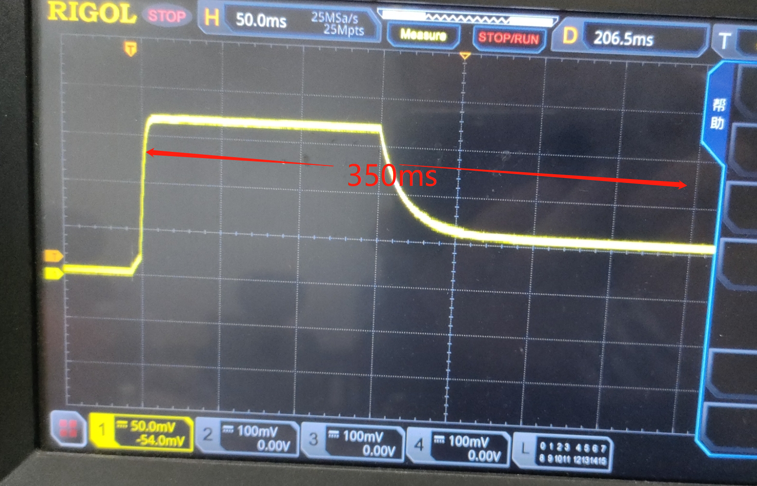
For SF32LB55x battery-voltage debugging, the upstream FAQ warns that readings in the first approximately 300 ms after startup or wake can be inaccurate because of RC charging and discharging; the observed waveform settles after about 350 ms. Add an appropriate sampling delay or discard the initial unstable samples. When measuring the divider node with a multimeter or oscilloscope, account for the measurement instrument's input impedance; the FAQ reports it can introduce an approximately 30 mV drop.
Bring-Up Check
Before adding multi-channel or cyclic acquisition, verify one channel with a stable, independently measured input:
- Confirm its target-family pad mapping and analog configuration.
- Confirm that the divider output stays within the target-family ADC limit.
- Compare the raw and calibrated results with the applied voltage.
- Retain the divider and calibration conditions with the board test record.
Official Source
- SF32LB52x ADC Usage and Configuration Guide
- SF32LB55x ADC Usage and Configuration Guide
- SF32LB56x ADC Usage and Configuration Guide
- SF32LB57x ADC Usage and Configuration Guide
- SF32LB58x ADC Usage and Configuration Guide
- SF32LB57x Hardware Design Guide — Storage & Manufacturing — GPADC pin assignment.
- OpenSiFli ADC FAQ — SF32LB55x factory calibration ranges and startup/wake validation.