SF32LB52x Hardware Design Guide — Schematic Design Guidelines
Part of the SF32LB52x Hardware Design Guide
Schematic Design Guidelines now spans three pages: this page (Sections 5.1-5.3: Minimum System, Power, and Clock), RF & User Interfaces (Sections 5.4-5.5), and Storage & Manufacturing (Sections 5.6-5.7). Start from the SF32LB52x Hardware Design Guide overview for device selection and the full design flow, or see the Schematic Checklist for the item-by-item review.
5. Schematic Design Guidelines
This chapter follows the schematic workflow across three pages. Complete the minimum-system review first, then expand into clock generation on this page; RF and user interfaces on the next page; and storage, manufacturing access, and PCB-dependent decisions on the final page. For each major block, confirm the design goal and variant scope before checking circuit requirements, pin assignment, common mistakes, and release checklist items.
| Block | Main Decision | Release Evidence |
|---|---|---|
| Minimum System Design | Exact variant, package, boot storage, bootstrap pins, debug/download access, and minimum bring-up path | Minimum-system review, bootstrap table, debug test points, boot and recovery plan |
| Power System | Variant power tree, charger path, BUCK, LDOs, boot-storage rail, operating modes, and wake sources | Power tree review, AVL parts, charger/OVP settings, low-power and wake-source plan |
| Clock Generation | 48 MHz and 32.768 kHz crystal selection, loading, and calibration assumptions | Crystal CL/ESR check, placement and routing screenshots, calibration plan |
| RF | RF matching, antenna path, and tuning access | RF impedance plan, matching-network placement screenshot, antenna tuning plan |
| User Interfaces | Display, audio, buttons, and vibration motor | Interface schematic review, timing/control pins, power sequencing, analog review |
| Storage and Connectivity | Boot medium, bootstrap pins, storage power switch, sensors, UART/I2C, and GPTIM | Bootstrap table, PA21 power control, bus assignment, storage rail review |
| Manufacturing | DBG_UART/SWD, test points, production flashing, calibration access, and release checklists | Test-point drawing, production fixture plan, completed release evidence |
5.1. Minimum System Design
Minimum system design is the first schematic release gate for an SF32LB52x board. It covers the decisions that must be correct before product peripherals are added: exact device variant, package, power tree, boot medium, bootstrap resistors, storage power control, debug/download access, clock sources, and wake behavior. A board can often tolerate late changes to display or sensor wiring; it usually cannot tolerate a wrong storage strap, missing debug access, unstable rail, or incompatible power-state assumption.
Use the following sequence for the first schematic pass:
- Select the exact device and package from Section 3.2 and Section 3.3.
- Choose the correct power path:
SF32LB520/3/5/7for rechargeable battery-powered products, or52B/D/E/G/Jfor externally regulated products. - Lock the power-system decisions in Section 5.2, including
VBUS/VBAT/VCCorPVDD/VDDIOA/VDD_SIP, BUCK, internal LDO decoupling, RF/audio rails, and all low-power load switches. - Select the boot medium and populate
PA13/PA17bootstrap pull options to match the boot table in Section 5.6.1. - Route all boot-storage power switches to
PA21, including large NOR Flash designs that must exit 4-byte mode after restart or Hibernate. - Reserve
PA18/PA19, ground, and a valid power reference for DBG_UART/SWD access before the enclosure and production fixture are frozen. - Select the 48 MHz and 32.768 kHz crystals from Section 5.3.1 and keep their placement constraints visible during schematic review.
- Assign wake pins, power-key behavior, charger events, and storage/sensor shutdown states before firmware low-power policy is finalized.
At the end of this gate, the schematic should be able to power up, boot from the selected medium, expose a recovery path, run clock calibration, and enter the intended low-power state without relying on optional product peripherals.
5.2. Power System
Power-system design defines the rails, load switches, charger path, OVP, internal LDO usage, wake behavior, and low-power states that make the minimum system reliable. Complete this section before PCB placement, because later display, storage, RF, audio, and sensor decisions depend on these rail assumptions.
5.2.1. Power Supply
Quick Summary
- Battery-powered devices use the
SF32LB520/3/5/7path withVBUS,VBAT,VCC, charging, and OVP decisions. - Regular-powered devices use the
52B/D/E/G/Jpath with externally regulatedPVDD,VDDIOA,VDD_SIP, and no internal charging path. - BUCK inductor, internal LDO decoupling, RF/audio rails, and standby load switches must be fixed before PCB placement.
Design Goal
Create a stable, low-leakage power tree that supports the selected variant, avoids overloading internal LDO outputs, keeps RF and audio rails quiet, and allows unused loads and boot storage to be switched off in low-power modes.
5.2.1.1. Processor Power Supply Requirements
| Pin | Min (V) | Typ (V) | Max (V) | Max Current (mA) | Description |
|---|---|---|---|---|---|
| VBUS | 4.6 | 5.0 | 5.5 | 500 | VBUS power input |
| VBAT | 3.2 | - | 4.7 | 500 | VBAT power output |
| VCC | 3.2 | - | 4.7 | 500 | System power input (1) |
| VSYS | - | 3.3 | - | 500 | VSYS power output (2) |
| BUCK_LX | - | 1.25 | - | 50 | BUCK output pin, connects to inductor |
| BUCK_FB | - | 1.25 | - | 50 | BUCK feedback / internal supply input, connects to the other end of the inductor plus an external capacitor |
| VDD_VOUT1 | - | 1.1 | - | 50 | Internal LDO, external capacitor, does not power peripherals |
| VDD_VOUT2 | - | 0.9 | - | 20 | Internal LDO, external capacitor, does not power peripherals |
| VDD_RET | - | 0.9 | - | 1 | Internal LDO, external capacitor, does not power peripherals |
| VDD_RTC | - | 1.1 | - | 1 | Internal LDO, external capacitor, does not power peripherals |
| VDD18_VOUT | - | 1.8 | - | 30 | SIP supply (3), internal, does not power peripherals; can be externally supplied when the LDO is disabled |
| VDD33_VOUT1 | - | 3.3 | - | 150 | 3.3 V LDO output 1 (4), no output by default; requires software configuration |
| VDD33_VOUT2 | - | 3.3 | - | 150 | 3.3 V LDO output 2, no output by default; requires software configuration |
| AVDD33_AUD | 2.97 | 3.3 | 3.63 | 50 | 3.3 V audio power input |
| AVDD_BRF | 2.97 | 3.3 | 3.63 | 100 | RF power input |
| MIC_BIAS | 1.4 | - | 2.8 | - | Microphone power output |
(1) VCC input, powered by a lithium battery: the default software low-battery threshold is 3.48 V. When powered from a constant-voltage supply, the supported range is 3.6–4.7 V, with 3.8 V recommended. (2) VSYS supplies power to AVDD_BRF. (3) VDD18_VOUT: SF32LB520U36 requires an external 3.3 V supply; SF32LB523/5/7Ux6 use the internal LDO and need no external supply. Configure the internal VDD18 LDO according to the chip model in software, and do not enable it when externally supplied. (4) VDD33_VOUT1: on SF32LB520U36 it only powers VDD18_VOUT, external Flash, and AVDD33_AUD; on SF32LB523/5/7Ux6 it only powers external Flash and AVDD33_AUD.
| Pin | Min (V) | Typ (V) | Max (V) | Max Current (mA) | Description |
|---|---|---|---|---|---|
| PVDD | 2.97 | 3.3 | 3.63 | 150 | PVDD system power input, 10 uF capacitor |
| BUCK_LX | - | 1.25 | - | 50 | BUCK output pin, connects to a 4.7 uH inductor |
| BUCK_FB | - | 1.25 | - | 50 | BUCK feedback / internal supply input, connects to the other end of the inductor plus a 4.7 uF capacitor |
| VDD_VOUT1 | - | 1.1 | - | 50 | Internal LDO, 4.7 uF capacitor, does not power peripherals |
| VDD_VOUT2 | - | 0.9 | - | 20 | Internal LDO, 4.7 uF capacitor, does not power peripherals |
| VDD_RET | - | 0.9 | - | 1 | Internal LDO, 0.47 uF capacitor, does not power peripherals |
| VDD_RTC | - | 1.1 | - | 1 | Internal LDO, 1 uF capacitor, does not power peripherals |
| VDDIOA | 1.71 | 1.8/3.3 | 3.63 | - | GPIO power input, 1 uF capacitor |
| AVDD33 | 2.97 | 3.3 | 3.63 | 100 | 3.3 V analog power input, 4.7 uF capacitor |
| AVDD33_AUD | 2.97 | 3.3 | 3.63 | 50 | 3.3 V audio power input, 2.2 uF capacitor |
| VDD_SIP | 1.71 | 1.8/3.3 | 3.63 | 30 | Internal LDO or external supply (1), 1 uF capacitor |
| AVDD_BRF | 2.97 | 3.3 | 3.63 | 100 | Analog power input, 4.7 uF capacitor |
| MIC_BIAS | 1.4 | - | 2.8 | - | Microphone power output, 1 uF capacitor |
(1) VDD_SIP: SF32LB52BU36 requires an external 1.8 V or 3.3 V supply; SF32LB52BU56 requires an external 3.3 V supply; SF32LB52DUB6 requires an external 1.8 V supply; SF32LB52E/G/JUx6 are powered directly by the internal LDO and need no external supply.
Hibernate mode note
When the system enters Hibernate mode, VDD_SIP must be switched off, otherwise there is a leakage risk on the I/O of the co-packaged storage. Use the dedicated PA21 pin to control the VDD_SIP power switch.
5.2.1.2. BUCK Inductor Selection
Both design groups use the same inductor specification.
Key Power Inductor Parameters
L (inductance) = 4.7 uH ± 20%, DCR (DC resistance) ≤ 0.4 Ω, Isat (saturation current) ≥ 450 mA.
5.2.1.3. Battery and Charging Control
There are two charging-circuit scenarios: an external charging management chip, or the on-chip integrated charging management module.
External Charging Management Chip
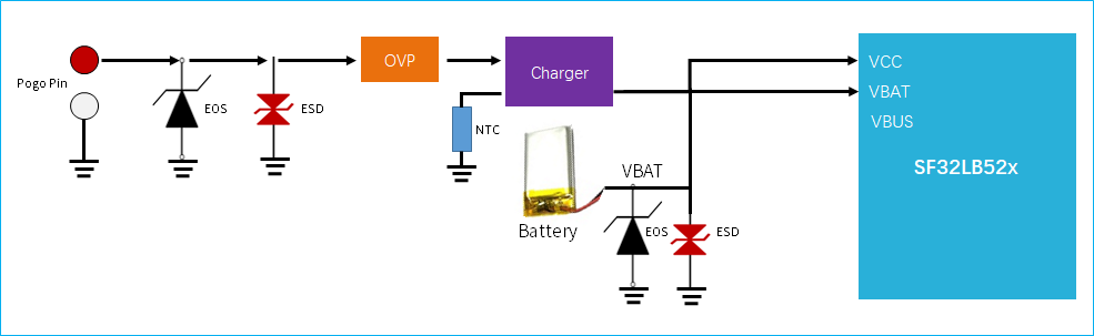
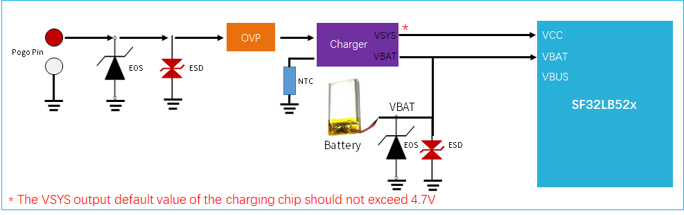
External charging chips come in two common types: without PPM (power path management) and with PPM. Without PPM, the battery directly supplies the VBAT and VCC pins. With PPM, the charger's VSYS supplies VCC, and the charger's VBAT connects to both the battery and the chip's VBAT pin. Both approaches measure battery voltage through the VBAT pin, which has an integrated GPADC channel with sampling accuracy within ±30 mV.
On-Chip Integrated Charging Management Module
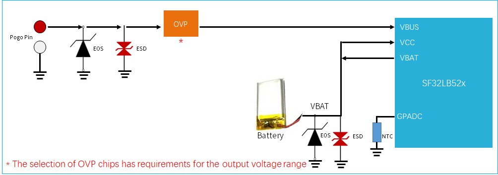
When using the integrated charging module, if the battery is low and the device is off, plugging in a charger requires the battery to charge up to the power-on threshold before the system can boot and display the charging screen.
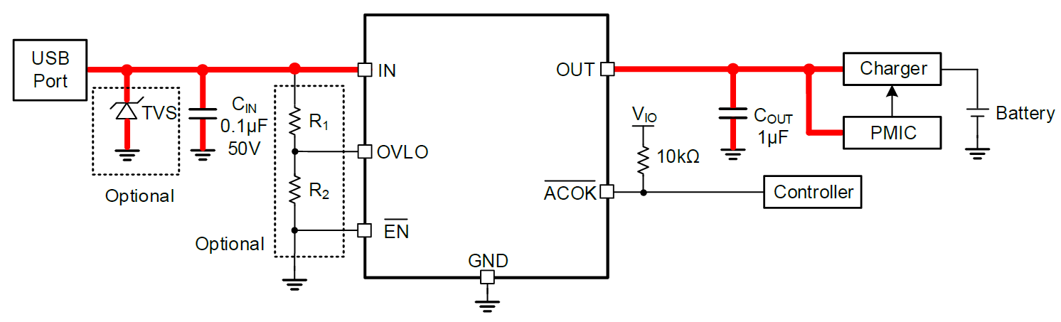
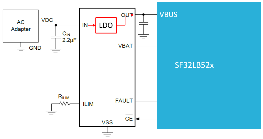
OVP Chip Selection (When Using the Integrated Charging Module)
The VBUS input range is 4.5 V–5.5 V, so choose one of these OVP chip types:
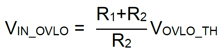
- Adjustable-OVLO OVP chip, e.g. AW32905FCR — set OVLO between 5.2 V and 5.5 V (VOVLO_TH tolerance ≤3%, resistor tolerance ≤1%)
- Regulated-output OVP chip, e.g. SGM4064YDE8G or LP5305AQVF — regulator output must be between 4.5 V and 5.5 V
Integrated Charging Module Notes
- VBUS input range: 4.6 V–5.5 V
- VCC input range: 3.2 V–4.7 V
- Default trickle current: 56 mA, trickle-to-constant-current transition voltage: 3.0 V
- Default constant charge current: 65 mA, adjustable 5–560 mA
- Default full-charge voltage: 4.2 V, adjustable up to 4.45 V
- Recharge voltage: full-charge voltage - 0.15 V
- The charger's VBUS must supply at least 350 mA; VBUS pin voltage must not drop below 4.6 V at maximum charge current
- For wireless charging, ensure the wireless charger's supply capability exceeds the constant charge current
Integrated LDO Notes
- Total capacitance on the VDD33_VOUT1 and VDD33_VOUT2 output paths must not exceed 9.6 uF
- AVDD33_AUD must be powered from VDD33_VOUT1, not from VSYS
- The LCD must not be powered from the internal LDO — use an external LDO
Not Applicable
The regular-powered variant is powered directly from a regulated external supply and has no charging management circuitry. This section does not apply. If your product needs battery power and charging, use the SF32LB520/3/5/7 series instead.
5.2.1.4. Reducing Standby Power
Recommended power structure: VDD33_VOUT2 supplies the vibration motor, VDD33_VOUT1 supplies external Flash and sensors, and the LCD uses an external LDO.
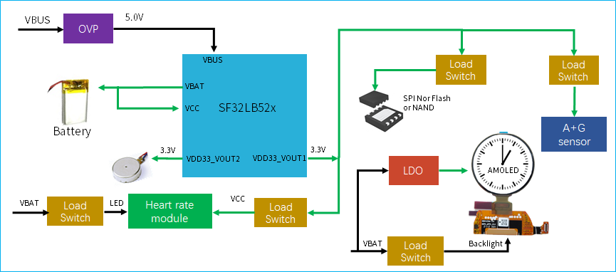
Control the default hardware state of power-switch GPIO pins carefully, and add megohm-range pull-up/pull-down resistors so load switches default to off. For LDO and load-switch selection, choose devices with low quiescent current (Iq) and low shutdown current (Istb), and pay particular attention to Iq on always-on power devices.
Use load switches for dynamic power management of each functional block; for always-on modules or paths, select devices with low quiescent current.
Control the default hardware state of power-switch GPIO pins carefully, and add megohm-range pull-up/pull-down resistors so load switches default to off. For LDO and load-switch selection, choose devices with low quiescent current (Iq) and low shutdown current (Istb), and pay particular attention to Iq on always-on power devices.
5.2.1.5. Power Design Checklist
- Confirmed which power variant (battery-powered / regular-powered) matches the exact chip model
- BUCK inductor meets 4.7 uH ±20%, DCR ≤0.4 Ω, Isat ≥450 mA
- All internal LDO decoupling capacitors are placed per requirements
- LCD power is isolated and not fed directly from the internal LDO
- Audio and RF power rails are properly filtered
- Battery-powered variant: charging path and OVP device voltage ranges verified; regular-powered variant: VDD_SIP/VDDIOA supply configured correctly for the chip model
Common Mistakes - Power
- Powering the LCD directly from an internal LDO instead of an external LDO.
- Mixing battery-powered and regular-powered supply assumptions in the same schematic.
- Leaving
VDD_SIPpowered during Hibernate on variants where storage leakage is a risk. - Choosing a charger or OVP device without verifying the worst-case VBUS current and voltage range.
Bring-Up Checks - Power
- Measure
VCC/PVDD, BUCK output, RF/audio rails, and storage supply before firmware enables peripherals. - Confirm charger attach, trickle charge, constant-current charge, and recharge behavior on battery-powered designs.
- Measure standby and Hibernate current with display, sensors, storage, and motor load switches off.
5.2.2. Operating Modes and Wake Sources
Quick Summary
- Active and Sleep retain fast interrupt response; DeepSleep and Standby trade wake time for lower current.
- Hibernate is the lowest-power state, but SRAM is not retained and some external supplies must be shut down.
- Wake-capable GPIO selection affects buttons, touch interrupt, charger events, and sensor wake behavior.
Design Goal
Select wake sources and external power-switch defaults so the product can enter the intended low-power state without leakage paths or missing wake events.
Shared Design
Operating modes and wake-source behavior apply across the SF32LB52x family unless a product-specific power tree intentionally disables an external wake source.
| Mode | CPU | Peripherals | SRAM | IO | LPTIM | Wake Source | Wake Time |
|---|---|---|---|---|---|---|---|
| Active | Run | Run | Accessible | Can toggle | Run | - | - |
| Sleep | Stop | Run | Accessible | Can toggle | Run | Any interrupt | <0.5 us |
| DeepSleep | Stop | Stop | Inaccessible, fully retained | Level held | Run | RTC, wake-up IO, GPIO, LPTIM, Bluetooth | 250 us |
| Standby | Reset | Reset | Inaccessible, fully retained | Level held | Run | RTC, wake-up IO, LPTIM, Bluetooth | 1 ms |
| Hibernate | Reset | Reset | Inaccessible, not retained | High-Z | Reset | RTC, wake-up IO | >2 ms |
The whole family supports 15 wake-capable interrupt sources in Standby and Hibernate modes:
| Wake Source | Pin | Wake Source | Pin |
|---|---|---|---|
| LWKUP_PIN0 | PA24 | LWKUP_PIN12 | PA36 |
| LWKUP_PIN1 | PA25 | LWKUP_PIN13 | PA37 |
| LWKUP_PIN2 | PA26 | LWKUP_PIN14 | PA38 |
| LWKUP_PIN3 | PA27 | LWKUP_PIN15 | PA39 |
| LWKUP_PIN10 | PA34 | LWKUP_PIN16 | PA40 |
| LWKUP_PIN11 | PA35 | LWKUP_PIN17 | PA41 |
| — | — | LWKUP_PIN18 | PA42 |
| — | — | LWKUP_PIN19 | PA43 |
| — | — | LWKUP_PIN20 | PA44 |
Operating-Mode Checklist
- Required wake pins are assigned before pin-mux is frozen.
- Pull states on wake pins are compatible with Standby and Hibernate.
- External storage and sensor supplies do not leak through I/O pins in Hibernate.
- Firmware and hardware teams agree which state is used for shipping, shelf, and normal standby modes.
5.3. Clock Generation
5.3.1. Crystal Selection
Quick Summary
- Use a 48 MHz main crystal and a 32.768 kHz RTC crystal.
- Favor low CL and low ESR parts from the AVL to reduce startup and static current.
- Keep crystal traces short, shielded, and away from heat, RF, charger, PMU, and DC/DC noise.
Design Goal
Provide stable, low-jitter clock sources while minimizing oscillator current, frequency drift, RF interference, and bring-up risk.
The chip requires two external clock sources: a 48 MHz main crystal and a 32.768 kHz RTC crystal. Requirements are identical for both variants.
Crystal Specification Requirements
| Crystal | Requirement | Notes |
|---|---|---|
| 48 MHz | 7 pF ≤ CL ≤ 12 pF (8.8 pF recommended), ΔF/F0 ≤ ±10 ppm, ESR ≤ 30 Ω (22 Ω recommended) | Lower CL and ESR reduce power consumption; matching capacitors are typically unnecessary when CL < 12 pF |
| 32.768 kHz | CL ≤ 12.5 pF (7 pF recommended), ΔF/F0 ≤ ±20 ppm, ESR ≤ 80 kΩ (38 kΩ recommended) | Lower CL and ESR reduce power consumption; matching capacitors are typically unnecessary when CL < 12.5 pF |
Recommended crystals:
| Part Number | Manufacturer | Parameters |
|---|---|---|
| E1SB48E001G00E | Hosonic | F0=48 MHz, ΔF/F0=-6~8 ppm, CL=8.8 pF, ESR≤22 Ω, TOPR=-30~85°C, 2016 metric package |
| SX20Y048000B31T-8.8 | TKD | F0=48 MHz, ΔF/F0=-10~10 ppm, CL=8.8 pF, ESR≤40 Ω, TOPR=-20~75°C, 2016 metric package |
| ETST00327000LE | Hosonic | F0=32.768 kHz, ΔF/F0=-20~20 ppm, CL=7 pF, ESR≤70 kΩ, TOPR=-40~85°C, 3215 metric package |
| SF32K32768D71T01 | TKD | F0=32.768 kHz, ΔF/F0=-20~20 ppm, CL=7 pF, ESR≤70 kΩ, TOPR=-40~85°C, 3215 metric package |
Additional Notes
The TKD SX20Y048000B31T-8.8 has a somewhat higher ESR, which slightly increases static power consumption. During PCB layout, remove the second-layer ground copper directly under the crystal to reduce parasitic load capacitance on the clock signal.
For the complete, continuously maintained qualification data, refer to the SiFli Approved Vendor List.
Common Mistakes - Clock
- Selecting a crystal only by frequency and package, without checking CL, ESR, tolerance, and temperature range.
- Placing the crystal near PA, charger, PMU, RF matching, or other heat/noise sources.
- Leaving copper or high-speed routing under the crystal keep-out region.
- Making 32 kHz traces long and parallel without spacing or ground shielding.
Clock Checklist
- 48 MHz and 32.768 kHz crystals match AVL/datasheet requirements.
- Crystal load capacitance and ESR are verified against the oscillator limits.
- Keep-out, trace length, trace width, spacing, and ground shielding are checked in PCB review.
- Bring-up plan includes measuring 48 MHz, 32 kHz, and Bluetooth frequency calibration behavior.
Continue to RF & User Interfaces.