SF32LB52x Hardware Design Guide — Design Review Checklist and References
Part of the SF32LB52x Hardware Design Guide
This page covers Sections 7-10: Design Review Checklist, Related Documents and References, Appendices, and Revision History. Return to PCB Layout Guidelines.
7. Design Review Checklist
- Minimum-system review is complete: exact variant, package, power tree, boot medium, bootstrap pins, debug/download access, clocks, and wake strategy are all documented
- The exact chip model and power variant are confirmed, and power schematics from the two variants are not mixed
- Processor power pins (VBUS/VBAT/VCC, or PVDD/VDDIOA/VDD_SIP) are within the datasheet voltage range
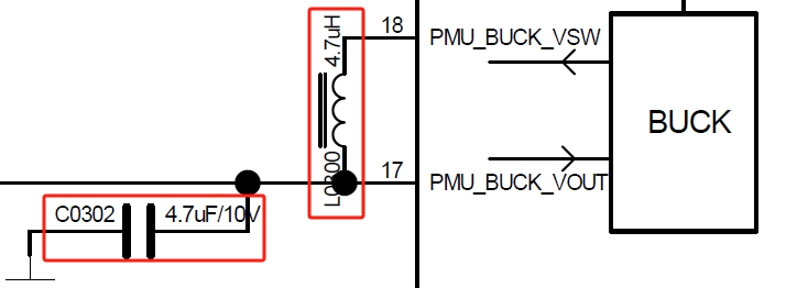
- BUCK inductor meets 4.7 uH ±20%, DCR ≤0.4 Ω, Isat ≥450 mA
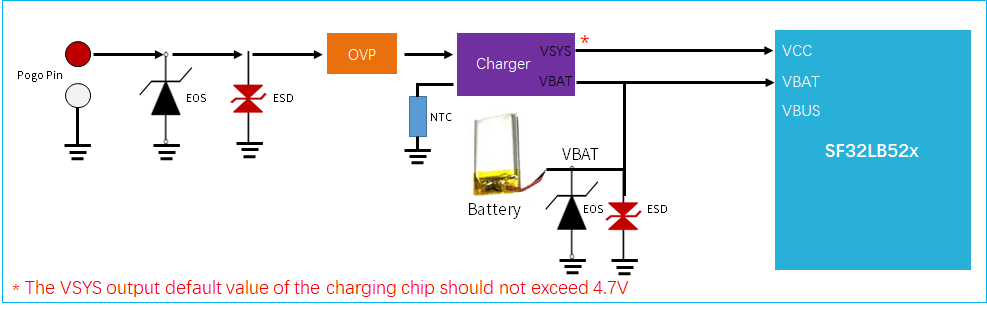
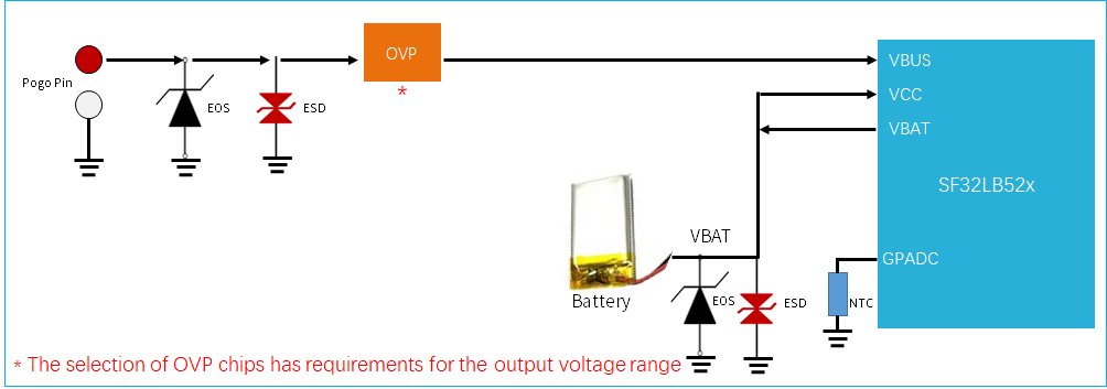
- Battery-powered variant: charging path, OVP device voltage range, and integrated-LDO output capacitance are verified
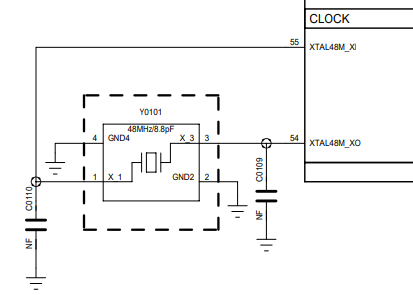
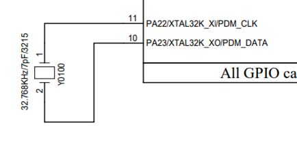
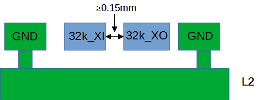
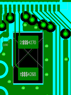
- 48 MHz and 32.768 kHz crystals meet the recommended specifications, with routing and keep-out zones satisfied
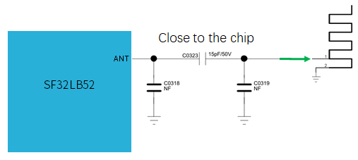
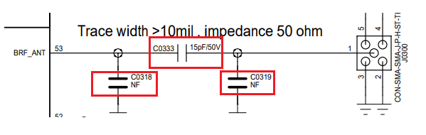
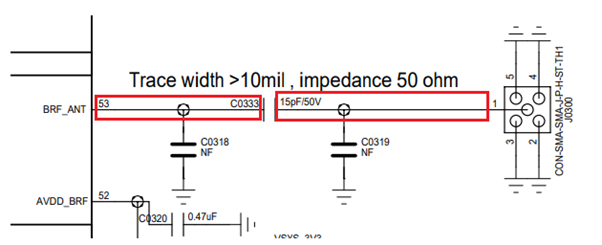
- RF trace is 50 Ω impedance, with the matching network placed close to the chip
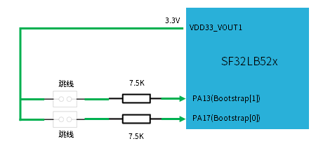
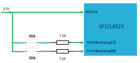
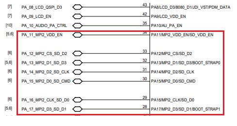
- Storage boot configuration (including the regular-powered variant's eMMC option) matches the Bootstrap pin settings
- Storage power switches are uniformly controlled through PA21, active high (on) / low (off)
- USB and SDIO differential trace impedance and length matching meet requirements
- DBG_UART/SWD multiplexed pins and production test points are reserved
- Key component part numbers have been verified against the latest SiFli Approved Vendor List
8. Related Documents and References
- SF32LB52x Datasheet (Official PDF)
- SF32LB52x User Manual (Official PDF)
- SF32LB52 Hardware Reference Design Package
- SF32LB520/3/5/7 Hardware Application Note (Source)
- 52B/D/E/G/J Hardware Application Note (Source)
- Local SiFli Approved Vendor List
- SiFli SF32LB52 Schematic & PCB Checklist (XLSX)
- SiFli Chip Hardware Design Guide Index (Wiki)
Additional source references:
- SF32LB52x Product Brief
- SF32LB52x Datasheet
- SF32LB52x Reference Manual
- SF32LB520/3/5/7 Hardware Application Note
- 52B/D/E/G/J Hardware Application Note
The Schematic Checklist (Section 5.8) and PCB Layout Checklist (Section 6.15) reproduce the same SF32LB52 Schematic & PCB Checklist (V1.0, 2026-01-21) item by item, alongside the schematic and PCB layout guidance they check against.
9. Appendices
The original SiFli application notes include the following schematic, PCB layout, mechanical, and power reference figures. These appendices preserve those source figures for review evidence, while Sections 5 and 6 remain the primary design guidance.
How to use these figures
Treat these figures as reference circuits and layout examples from the source application notes. Use the rule text, tables, datasheet, reference manual, latest reference design package, and AVL to confirm the final implementation for the exact device and product.
| Need | Start Here |
|---|---|
| Smart watch block-diagram examples for both SF32LB52x design groups | Appendix A: A Typical Smart Watch Application |
| Circuit-level schematic examples for RF, storage/boot, buttons, motor, audio, clock, USB, and DC/DC | Appendix B: Reference Schematics |
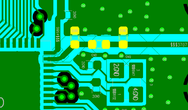
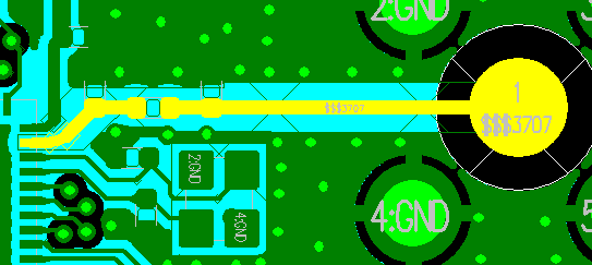
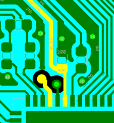
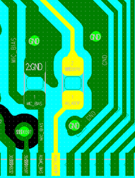
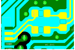
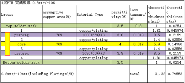
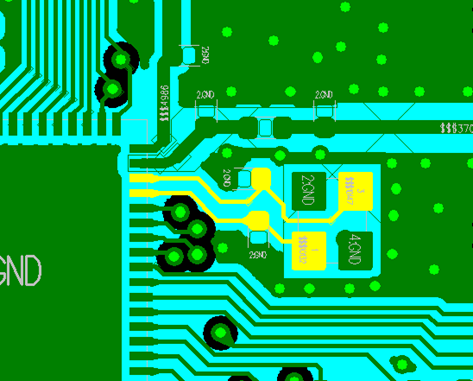
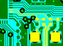
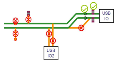
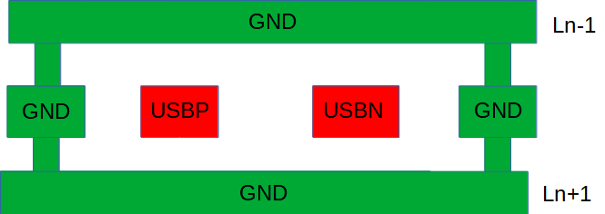
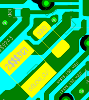
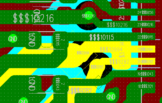
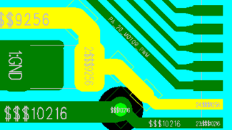
| PCB placement and routing examples for RF, storage, audio, stack-up, fanout, clock, USB, and DC/DC | Appendix C: Reference PCB Layouts |
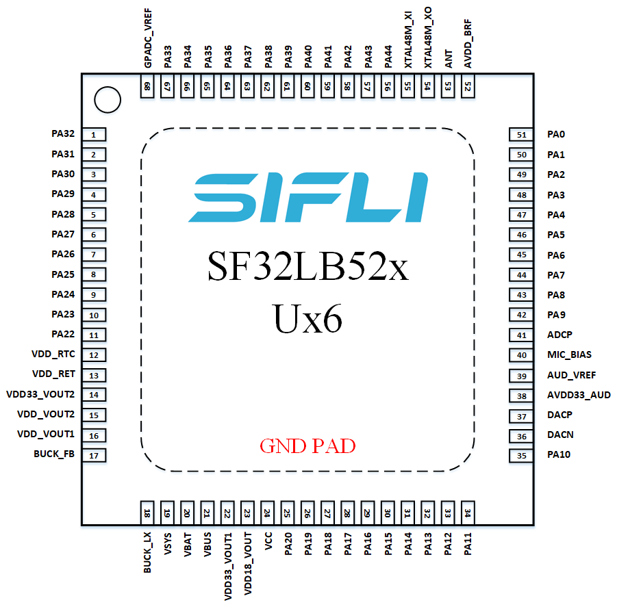
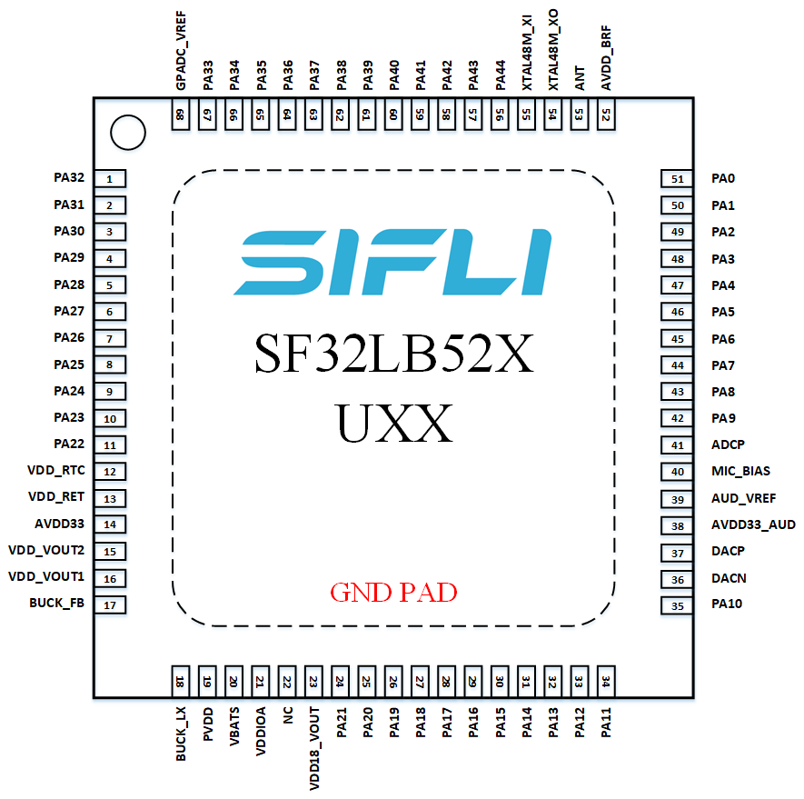
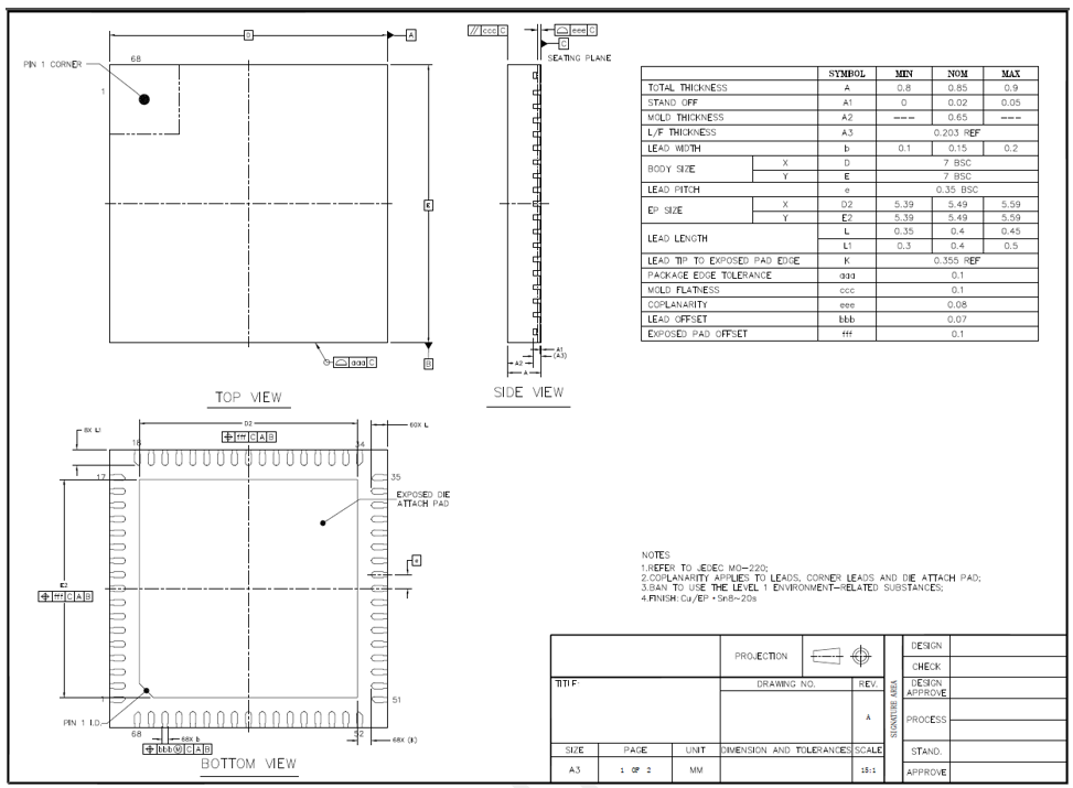
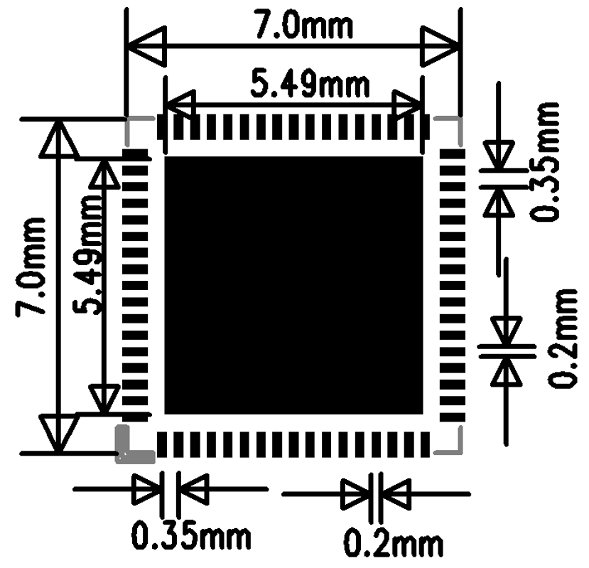
| Package outline, shape, and land-pattern drawings | Appendix D: Mechanical |
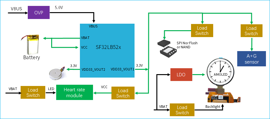
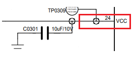
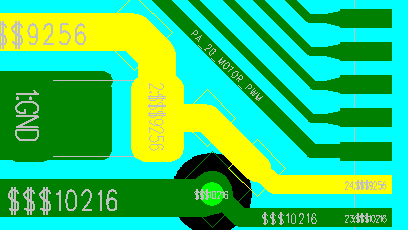
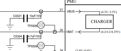
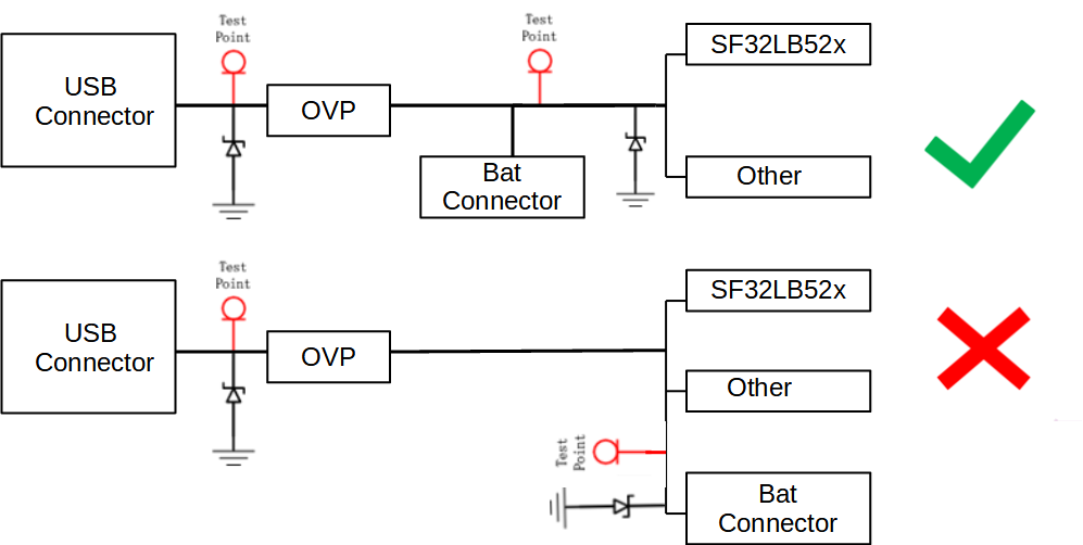
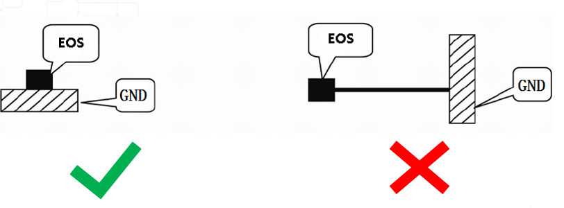
| Charging, OVP, power-tree, and PMU reference circuits and layouts | Appendix E: Power |
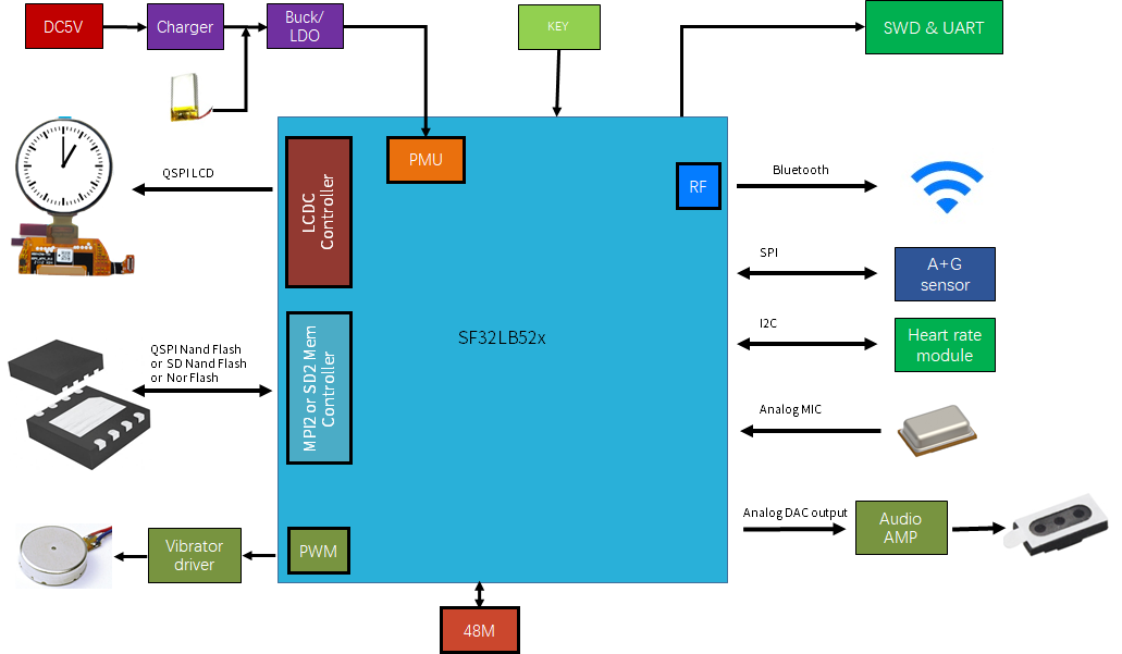
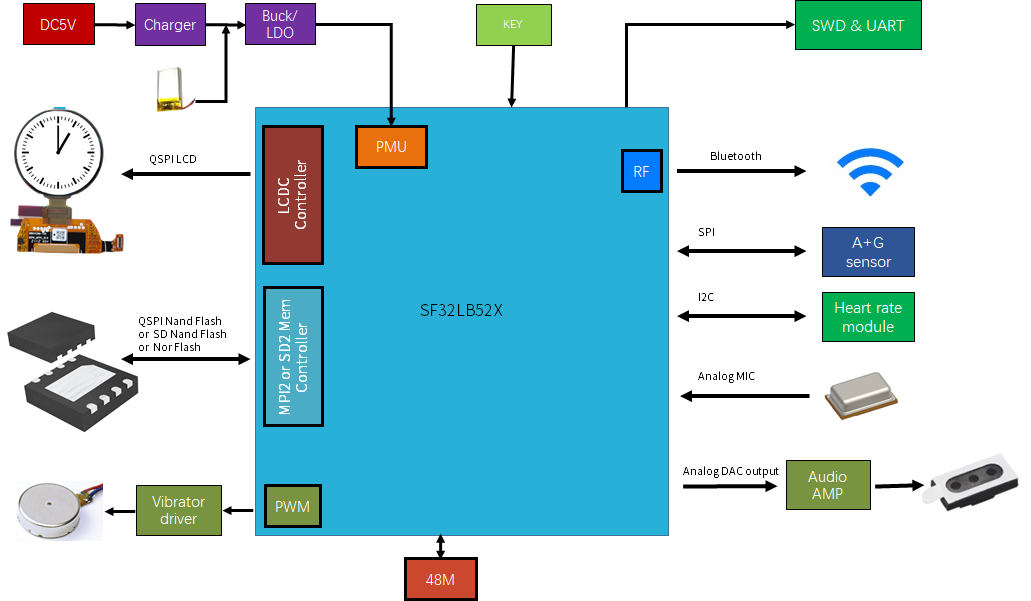
Appendix A. A Typical Smart Watch Application
A typical SF32LB52x smart watch design includes the MCU, display, touch controller, storage, sensors, vibration motor, audio input/output, Bluetooth antenna, clock sources, power management, debug access, and production-test access. The battery-powered design additionally includes charging management.
Appendix B. Reference Schematics
RF
Storage and Boot
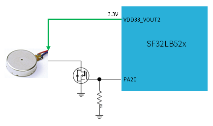
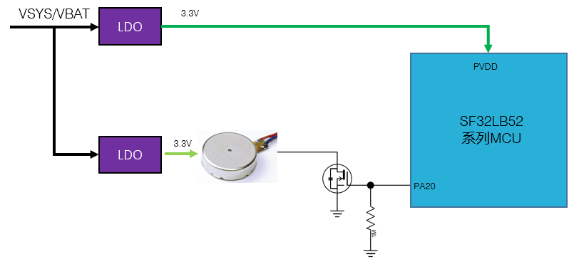
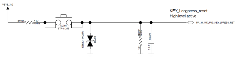
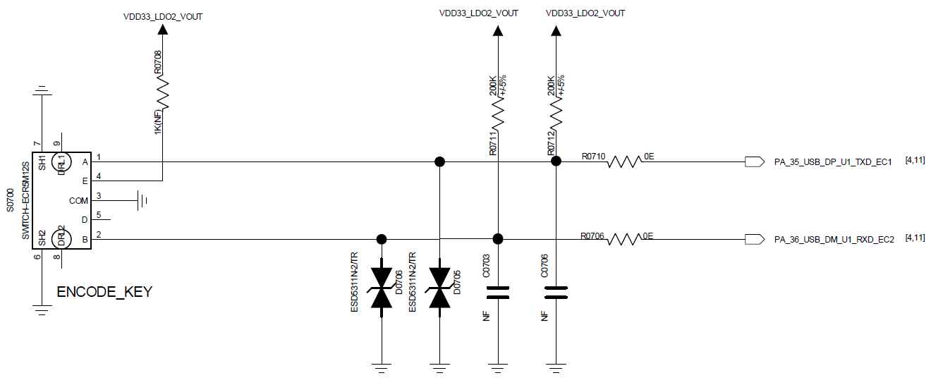
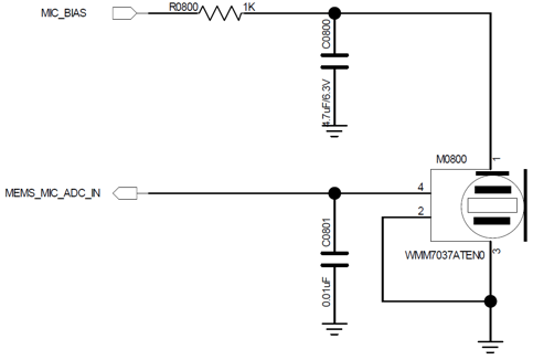
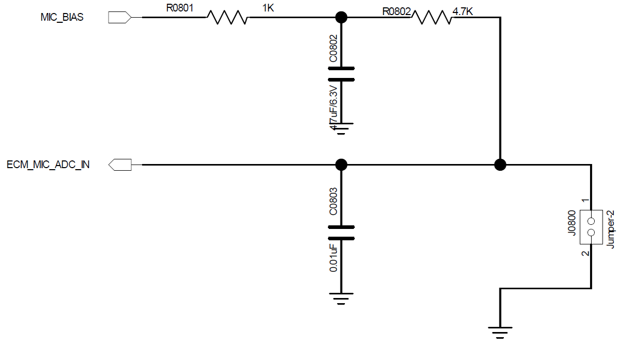
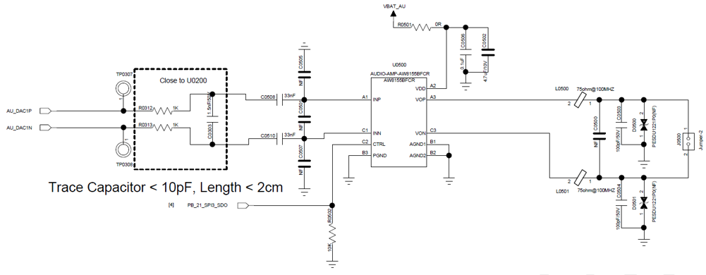
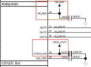
Buttons, Motor, and Audio
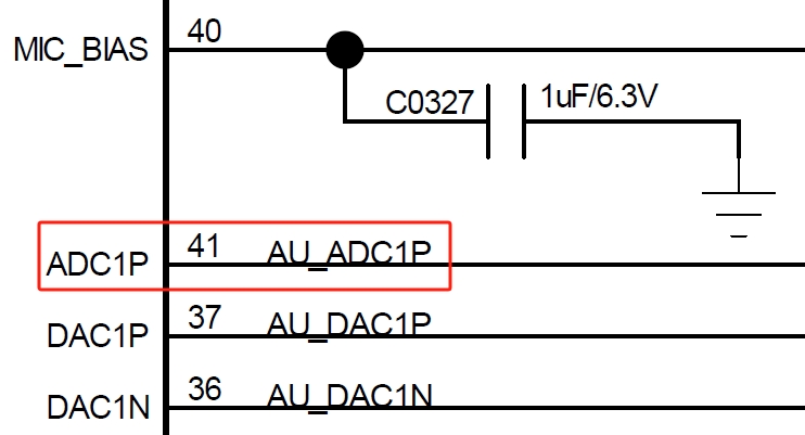
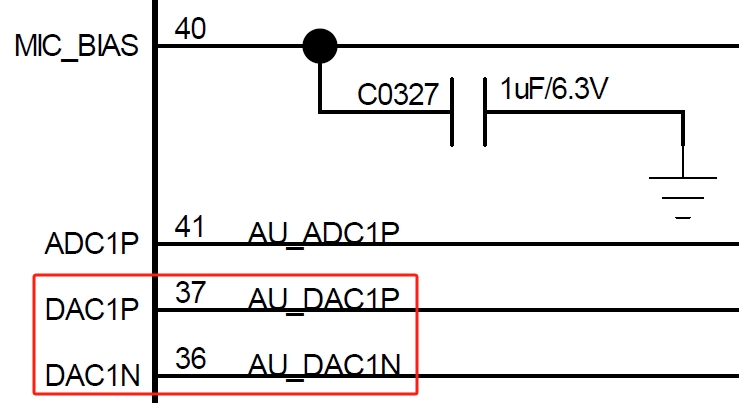
Clock
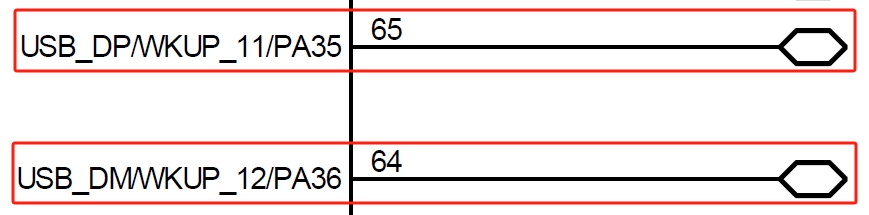
USB
DC/DC
Appendix C. Reference PCB Layouts
RF
Storage

Audio
PCB Foundation
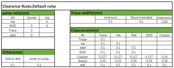
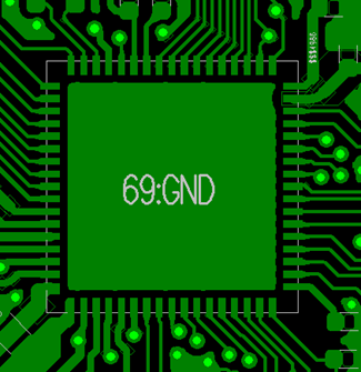
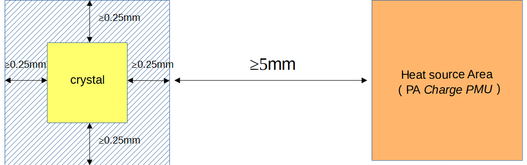
Clock Routing
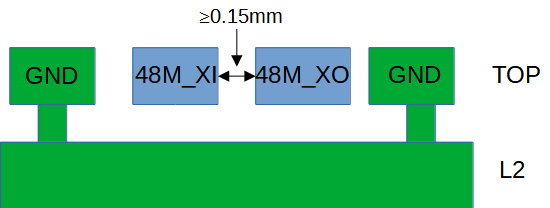
USB
DC/DC
Appendix D. Mechanical

Appendix E. Power
SF32LB520/3/5/7 (Battery-Powered)
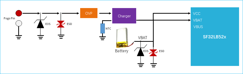

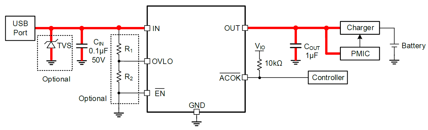
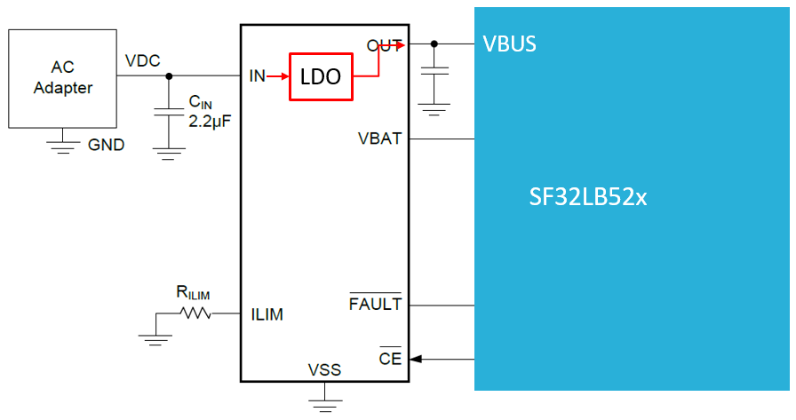
52B/D/E/G/J (Regular-Powered)
10. Revision History
| Version | Date | Note |
|---|---|---|
| 1.1 | 2026-07 | Promoted Power System to a peer schematic section, split Clock Generation and RF into separate schematic sections, and renumbered the following schematic guidance sections. |
| 0.0.1 | 10/2024 | Original release of SF32LB520-3-5-7-HW-Application |
| 0.0.1 | 10/2024 | Original release of SF32LB52B-E-G-J-HW-Application |
| 1.0 | This document | Combined both official hardware application notes into a single guide, using tabs to separate battery-powered vs. regular-powered variant content |
10.1. Checklist Revision History
The item-by-item checklist in the Schematic Checklist and PCB Layout Checklist is versioned separately from the guide, following SiFli's own SF32LB52 Schematic & PCB Checklist spreadsheet.
| Version | Date | Note |
|---|---|---|
| 1.0 | 2026-01-21 | Initial release, based on SiFli's SF32LB52 Schematic & PCB Checklist V1.0 |