SF32LB52x Hardware Design Guide — RF & User Interfaces
Part of the SF32LB52x Hardware Design Guide
This page covers Sections 5.4-5.5 of Schematic Design Guidelines: RF and User Interfaces. Return to Minimum System, Power & Clock, continue to Storage & Manufacturing, or see the Schematic Checklist for the item-by-item review.
5.4. RF
5.4.1. RF Schematic and Antenna Path
Quick Summary
- Route the antenna path as a 50 Ω controlled-impedance trace.
- Reserve a π matching network even if the selected antenna is already matched.
- Keep the RF path short, shielded, and isolated from crystal, DC/DC, display, and charger noise.
Design Goal
Maximize Bluetooth sensitivity and radiated performance by preserving impedance control, minimizing discontinuities, and leaving enough matching flexibility for final antenna tuning.
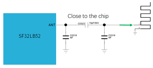
RF trace characteristic impedance is 50 Ω. If the antenna is already matched, no additional RF components are required, but a reserved π-type matching network is still recommended for spurious filtering or antenna tuning.
5.4.2. RF Review and Tuning
Common Mistakes - RF
- Placing the matching network near the antenna instead of close to the chip-side RF pin.
- Routing RF through unnecessary vias or sharp bends.
- Sharing noisy ground return paths with DC/DC, display, USB, or charger circuits.
- Omitting the matching reserve and leaving no practical antenna-tuning path.
RF Checklist
- RF trace impedance target is defined with the PCB vendor.
- Pi matching network is reserved and placed close to the chip.
- Ground-via fence and RF keep-out are reviewed.
- Antenna tuning and certification access are planned before enclosure freeze.
5.5. User Interfaces
5.5.1. Display
Quick Summary
- Supported interfaces include SPI, Dual-SPI, Quad-SPI, serial JDI, and EPD on supported regular-powered variants.
- Maximum documented display resolution is 512 x 512.
- Reset, TE, backlight PWM, touch I2C, touch interrupt, and display power sequencing should be reviewed together.
Design Goal
Select a display interface that meets bandwidth and power targets while preserving wake, reset, backlight, and touch behavior across normal operation and low-power states.
The chip supports 3-Line SPI, 4-Line SPI, Dual-data SPI, Quad-data SPI, and serial JDI interfaces, with 16.7M-color (RGB888), 262K-color (RGB666), 65K-color (RGB565), and 8-color (RGB111) depth modes, up to 512x512 resolution.
Supported LCD driver models:
| Model | Manufacturer | Resolution | Type | Interface |
|---|---|---|---|---|
| RM69090 | Raydium | 368x448 | AMOLED | 3/4-Line SPI, Dual/Quad-data SPI, MIPI-DSI |
| RM69330 | Raydium | 454x454 | AMOLED | 3/4-Line SPI, Dual/Quad-data SPI, 8-bit 8080 MCU, MIPI-DSI |
| ILI8688E | ILITEK | 368x448 | AMOLED | Quad-data SPI, MIPI-DSI |
| SH8601A | Shine World Technology | 454x454 | AMOLED | 3/4-Line SPI, Dual/Quad-data SPI, 8-bit 8080 MCU, MIPI-DSI |
| SPD2012 | Solomon | 356x400 | TFT | Quad-data SPI |
| GC9C01 | Galaxycore | 360x360 | TFT | Quad-data SPI |
| GC9B71 | Galaxycore | 320x380 | TFT | Quad-data SPI |
| ST77903 | Sitronix | 400x400 | TFT | Quad-data SPI |
| ICNA3311 | Chipone | 454x454 | AMOLED | Quad-data SPI |
| FT2308 | FocalTech | 410x494 | AMOLED | Quad-data SPI |
5.5.1.1. SPI/QSPI Display Interface
| SPI Signal | Pin | Description |
|---|---|---|
| CSx | PA03 | Chip select |
| WRx_SCL | PA04 | Clock |
| DCx | PA06 | Data/command in 4-wire SPI; data 1 in Quad-SPI |
| SDI_RDx | PA05 | Data input in 3/4-wire SPI; data 0 in Quad-SPI |
| SDO | PA05 | Data output in 3/4-wire SPI; short together with SDI_RDx |
| D[0] | PA07 | Data 2 in Quad-SPI |
| D[1] | PA08 | Data 3 in Quad-SPI |
| RESET | PA00 | Display reset |
| TE | PA02 | Tearing-effect signal to MCU |
5.5.1.2. JDI Display Interface
| JDI Signal | I/O | Description |
|---|---|---|
| JDI_VCK | PA39 | Shift clock for the vertical driver |
| JDI_VST | PA08 | Start signal for the vertical driver |
| JDI_XRST | PA40 | Reset signal for horizontal and vertical drivers |
| JDI_HCK | PA41 | Shift clock for the horizontal driver |
| JDI_HST | PA06 | Start signal for the horizontal driver |
| JDI_ENB | PA07 | Write enable signal for pixel memory |
| JDI_R1 | PA05 | Red image data (odd pixels) |
| JDI_R2 | PA42 | Red image data (even pixels) |
| JDI_G1 | PA04 | Green image data (odd pixels) |
| JDI_G2 | PA43 | Green image data (even pixels) |
| JDI_B1 | PA03 | Blue image data (odd pixels) |
| JDI_B2 | PA02 | Blue image data (even pixels) |
5.5.1.3. EPD Display Interface
The chip supports an 8-bit parallel EPD display interface:
| EPD Signal | I/O | Description |
|---|---|---|
| CLK | PA04 | Clock source driver |
| CKV/CPV | GPIO | Clock gate driver |
| SPH | PA06 | Start pulse source driver |
| SPV/STV | GPIO | Start pulse gate driver |
| LE | GPIO | Latch enable source driver |
| OE | GPIO | Output enable source driver |
| D0–D7 | PA07/PA08/PA37/PA39/PA40/PA41/PA42/PA43 | Data signal source driver, bits 0–7 |
| GMODE | GPIO | Output mode selection, gate driver |
| VPOS/VNEG | TPS | Positive/negative power supply, source driver |
| VGH/VGL | TPS | Positive/negative power supply, gate driver |
| VCOM | TPS | Common connection |
| TPS_WAKEUP/TPS_PWRUP | GPIO | TPS PMIC wake-up / power-up control |
| TPS_SDA/TPS_SCL | I2C | TPS PMIC I2C interface |
| TPS_PWRCOM | GPIO | TPS PMIC VCOM_CTRL, VCOM enable |
| TPS_GOOD | GPIO | TPS PMIC power-good output |
Note
Signals marked "PA**" must use the fixed IO assignment shown. Signals marked GPIO can be assigned to any IO. Signals marked TPS come from the display PMIC (TPS) output to the panel. Signals marked I2C require an IO with I2C capability.
Not Applicable
SiFli's official SF32LB520/3/5/7 hardware application note does not include an EPD parallel-interface reference design. If your product needs EPD display support, consult the 52B/D/E/G/J documentation and confirm feasibility for the battery-powered variant with SiFli FAE support directly.
5.5.1.4. Touch and Backlight Interface
The SF32LB52x supports an I2C touch-controller interface with a touch-status interrupt input, plus one PWM signal for backlight enable and brightness control.
| Touch/Backlight Signal | Pin | Description |
|---|---|---|
| Interrupt | PA43 | Touch status interrupt (wake-capable) |
| I2C1_SCL | PA42 | Touch I2C clock |
| I2C1_SDA | PA41 | Touch I2C data |
| BL_PWM | PA01 | Backlight PWM control |
| Reset | PA44 | Touch controller reset |
Common Mistakes - Display
- Forgetting reset, TE, backlight PWM, or touch interrupt pins during pin assignment.
- Assuming EPD support on the battery-powered variant without confirming the actual device and source design.
- Powering the display from an internal LDO rather than an appropriately sized external rail.
- Routing display clocks and data beside crystal, RF, audio, or high-impedance analog nodes.
Display Checklist
- Display interface, color depth, resolution, and bandwidth match the selected panel.
- Reset, TE, backlight PWM, touch I2C, and touch interrupt are assigned and documented.
- Display power rail and sequencing are compatible with standby and wake behavior.
- Bring-up plan covers reset, panel ID/readback where available, backlight, touch interrupt, and first image.
5.5.2. Audio Interface
Quick Summary
- The analog microphone input is single-ended and requires a DC-blocking capacitor.
- The DAC output is differential and should be routed as a short, shielded differential pair.
- Audio power filtering and MIC_BIAS placement strongly affect noise performance.
Design Goal
Preserve analog signal quality by keeping microphone, DAC, bias, and audio power paths short, filtered, shielded, and isolated from digital and switching-noise sources.
The shared audio interface provides:
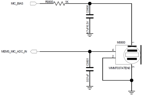
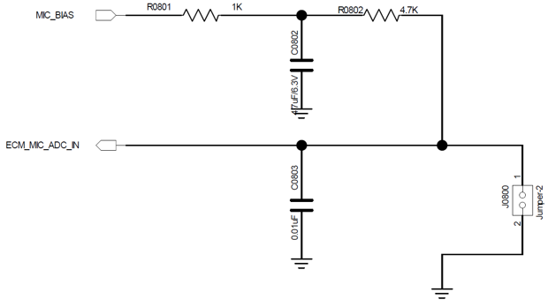
- One single-ended ADC input for an analog microphone, with a DC-blocking capacitor of at least 2.2 uF in series; the microphone is powered from the chip's MIC_BIAS output
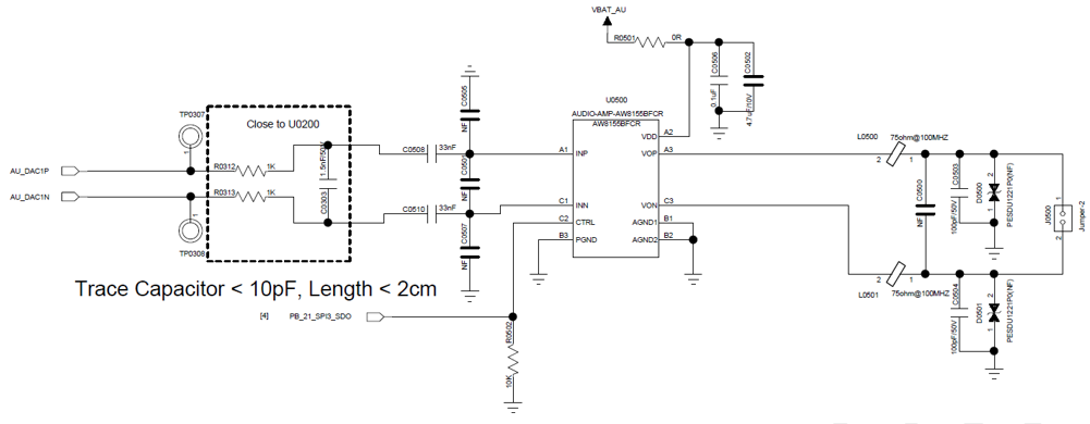
- One differential DAC output for an external audio PA — route as a differential pair with proper ground shielding; keep trace capacitance < 10 pF and length < 2 cm
| Audio Signal | Pin | Description |
|---|---|---|
| BIAS | MIC_BIAS | Microphone power |
| AU_ADC1P | ADCP | Single-ended analog microphone input |
| AU_DAC1P | DACP | Differential analog output, positive |
| AU_DAC1N | DACN | Differential analog output, negative |
Common Mistakes - Audio
- Routing microphone or DAC traces near display clocks, DC/DC, RF, USB, or SDIO.
- Placing MIC_BIAS or AVDD33_AUD filter capacitors far from the chip pins.
- Treating DACP/DACN as independent single-ended signals instead of a differential pair.
- Allowing high parasitic capacitance or long trace length on the analog output.
Audio Checklist
- MIC_BIAS, ADCP, DACP, and DACN component placement is reviewed against the layout examples.
- DACP/DACN are routed as a short, shielded differential pair.
- Audio filter capacitors are close to their pins and grounded cleanly.
- Bring-up plan covers microphone bias, ADC noise floor, DAC output, PA enable, and audible noise.
5.5.3. Buttons
Quick Summary
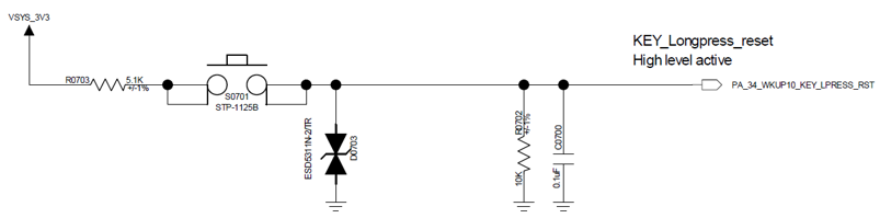
PA34supports the power button, power on/off behavior, and long-press reset.- Rotary encoder buttons should follow the reference circuit and be reviewed together with wake, debounce, and ESD requirements.
Design Goal
Provide reliable user-input and reset behavior without false wake events, stuck reset states, or high standby leakage through pull networks.
5.5.3.1. Power Button
PA34 supports long-press reset and can be designed as a combined power on/off and long-press-reset button. The long-press reset function is active-high, so the default state should be pulled low and driven high when the button is pressed.
5.5.3.2. Mechanical Rotary Encoder Button
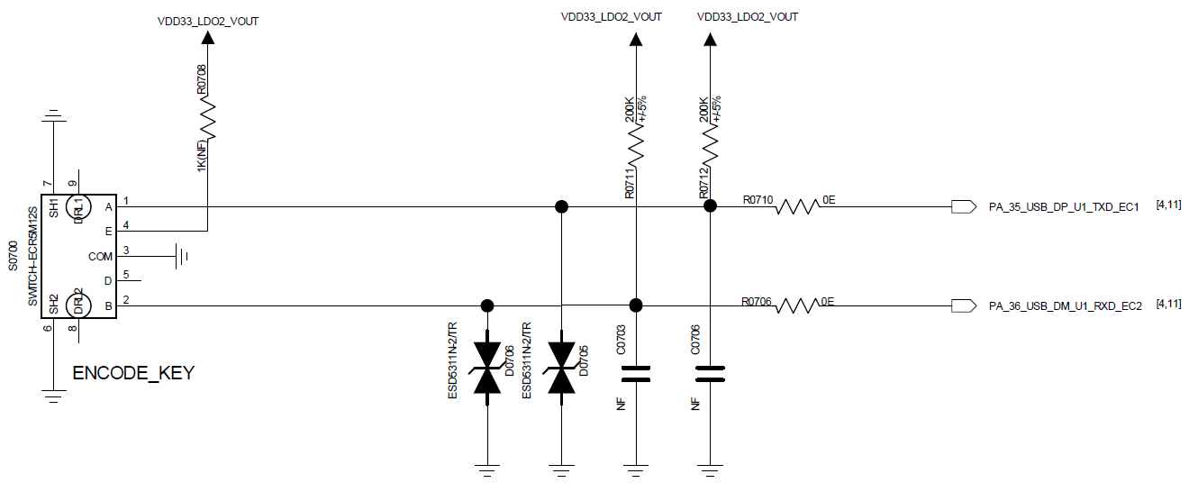
Use the reference design as the baseline for the rotary encoder button circuit.
Common Mistakes - Buttons
- Leaving
PA34floating or biased to the wrong default level. - Forgetting that button circuits may need wake, ESD, debounce, and production-test access.
- Sharing button nets with noisy or heavily loaded functions without checking wake reliability.
Button Checklist
- Power/long-press-reset default level is correct.
- Wake behavior is verified for the intended low-power states.
- ESD and mechanical debounce requirements are reviewed.
- Bring-up plan includes short press, long press, wake, and reset behavior.
5.5.4. Vibration Motor
Quick Summary
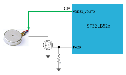
- Use a PWM output to drive the vibration motor through an external driver stage.
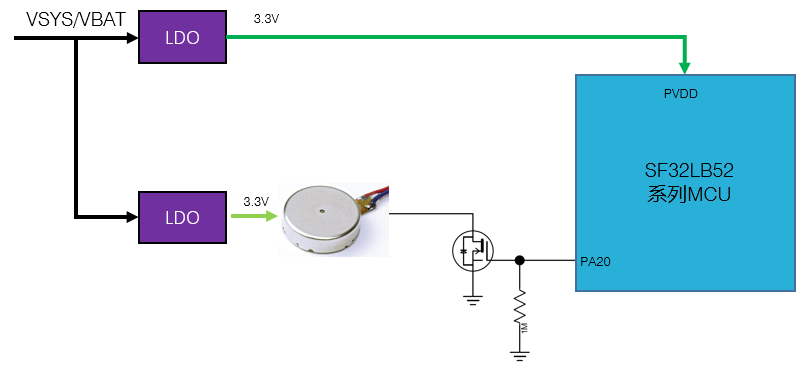
- Power the motor from a switchable rail where standby current matters.
Design Goal
Deliver repeatable haptic feedback while keeping motor surge current, switching noise, and standby leakage away from sensitive rails and wake circuits.
The SF32LB52x supports a PWM output for driving a vibration motor through an external driver stage.
Motor Checklist
- Motor driver, flyback/ESD protection, and supply current rating are reviewed.
- Motor rail default state is off in standby and shipping states.
- PWM pin assignment does not conflict with display, storage, or debug pins.
- Bring-up plan covers PWM duty sweep, start current, audible noise, and standby leakage.